22 min read Hugues Orgitello EN
PCI Express: generations, lanes, signal integrity
PCI Express guide: x1-x16 lane architecture, PCIe 3.0-6.0, bandwidth, backward compatibility and industrial integration. AESTECHNO Montpellier.
PCIe: the backbone of high-performance systems
PCI Express (PCIe) is the point-to-point serial bus that has become the backbone of modern high-performance electronic systems. It connects critical components - NVIDIA or AMD GPUs, NVMe SSDs, FPGAs (Xilinx/Intel), Intel Xeon SoCs and expansion cards - with throughput ranging from 250 MB/s per lane (PCIe 1.0) to 8 GB/s per lane (PCIe 6.0).
Most high-performance electronics projects involve a PCIe interface. After integrating PCIe links into many custom motherboards over more than 10 years - real-time acquisition systems, embedded AI platforms, edge-computing servers - we have watched this technology jump from 2.5 GT/s (PCIe 1.0) to 64 GT/s (PCIe 6.0), a 25x multiplier in less than 20 years.
TL;DR
- Peripheral Component Interconnect Express (PCIe) is a point-to-point serial bus maintained by the PCI Special Interest Group (PCI-SIG), which specifies the physical, link and transaction layers from PCIe 1.0 through PCIe 6.0.
- Each generation doubles the per-lane throughput: PCIe 3.0 = 8 Gigatransfers per second (GT/s), PCIe 4.0 = 16 GT/s, PCIe 5.0 = 32 GT/s, PCIe 6.0 = 64 GT/s using Pulse Amplitude Modulation 4 (PAM4) and Flow Control Unit (FLIT) encoding.
- Documented in the official architecture guides from Intel and AMD (Intel PCIe architecture, AMD developer hub), PCIe 5.0 is the de facto standard for datacenter and workstation platforms in 2026.
- On our test bench we have measured a 20 to 30 % gain in vertical eye-diagram opening simply by applying systematic back-drilling to PCIe Gen 4 vias running at 16 GT/s.
PCI Express (Peripheral Component Interconnect Express) is a point-to-point serial bus interface used to connect high-performance internal components such as GPUs, NVMe SSDs and expansion cards. Unlike older parallel buses, PCIe relies on independent lanes that deliver up to 8 GB/s per lane in version 6.0, with low latency and guaranteed backward compatibility.
At AESTECHNO, we design and integrate custom PCIe systems for industrial, medical and AI applications. Our expertise covers high-speed routing, signal-integrity constraints and EMC certification - all critical when a single PCIe x16 link can carry up to 128 GB/s of data.
In this article we share what we have learned in the lab: PCIe architecture and lanes, the evolution of the spec, the design pitfalls to avoid, and our recommendations for picking the right generation for a given application.
Project with a PCIe interface?
Our engineers analyse your requirements and recommend the optimal architecture: PCIe 4.0/5.0/6.0, lane count, routing constraints.
Free 30-minute audit - response within 24 h
PCIe generations compared: from 1.0 to 6.0
The PCIe generation comparison is essentially a lookup table linking per-lane throughput, x16 aggregate bandwidth and typical workloads. Per the PCI-SIG, every new generation doubles the per-lane data rate of the previous one while preserving full backward compatibility.
| Version | Per lane | x16 aggregate | Typical workload |
|---|---|---|---|
| PCIe 3.0 | 1 GB/s | 16 GB/s | Mid-range GPU, mainstream SSD |
| PCIe 4.0 | 2 GB/s | 32 GB/s | High-end GPU, Gen4 NVMe |
| PCIe 5.0 | 4 GB/s | 64 GB/s | Datacenter, AI/HPC, Gen5 NVMe |
| PCIe 6.0 | 8 GB/s | 128 GB/s | Hyperscale cloud, AI accelerators |
Our recommendation: for any new design starting in 2025, target PCIe 4.0 as a minimum. PCIe 5.0 is becoming the standard for bandwidth-hungry workloads (AI training, large-scale storage). PCIe 6.0 is still confined to hyperscale datacenters.
PCIe lab case studies
Our hands-on PCIe experience covers many critical configurations. Here are three representative cases that illustrate the signal-integrity and stack-up trade-offs we routinely face:
- Case 1: PCIe Gen 4, post-layout eye closure caused by an un-back-drilled via stub. At 16 GT/s, a residual 0.5 mm stub creates a resonance inside the useful band and collapses the horizontal margin. Counter to the reflex of swapping the laminate, we first push for systematic back-drilling of the differential-lane transition vias, with a typical 20 to 30 % gain in vertical eye opening.
- Case 2: industrial Intel i5 platform with a heavy PCIe footprint (up to 16 combined Gen 4 / Gen 5 lanes) feeding accelerators and NVMe storage. Stack-up choice is structural here: we favour a hybrid build with high-Tg FR-4 for power and digital layers and a Megtron 6 core for the layers carrying the PCIe lanes. Contrary to the assumption that Gen 5 mandates exotic Tachyon-class material, a clean Megtron 6 design holds up on short Gen 5 links (under 10 cm of cumulative trace).
- Case 3: industrial qualification to IPC-6012 Class 2. On long-life industrial products, PCIe lanes must survive aggressive thermal cycling. We specify IPC-6012 Class 2, with localised Class 3 reinforcement on critical vias in the highest-density zones.
PCIe tooling, standards and materials
Our PCIe methodology rests on a precise set of standards: the PCI-SIG Base Specification v4.0 and v5.0 for the electrical and protocol layers, JEDEC SFF (EDSFF E1.S/E3.S) for the M.2 / U.2 / EDSFF form factors, IPC-6012 Class 2/3 for PCB qualification and IPC-2221/2222 for design rules. As specified by PCI-SIG in v6.0, PAM4 + FLIT encoding reaches 64 GT/s without doubling the Nyquist frequency. On the operating-system side, the Linux kernel PCI documentation (kernel.org) describes PCIe enumeration and Active State Power Management (ASPM). The PCI Express article on Wikipedia offers a thorough generational history, while the IEEE 802.3 family published by IEEE formalises the network pairings often co-integrated with PCIe (e.g. 100 GbE SmartNICs). For industrial connectivity we routinely work with Samtec high-speed connectors and Quectel modules in extended M.2 form factors.
Material selection follows a clear hierarchy keyed to the target generation: high-Tg FR-4 is acceptable up to PCIe Gen 3, Isola I-Speed or 370HR/IS410 for production-grade Gen 3 / Gen 4 builds, Megtron 6 for nominal Gen 4 / Gen 5, and Megtron 7 or Tachyon 100G for long Gen 5 and Gen 6 links. On the validation side we run ANSYS SIwave in post-layout for S-parameter extraction, crosstalk analysis and eye-diagram generation before release to fab. That step has caught more than one via stub or impedance discontinuity that the Altium DRC let through.
Contrary to the belief that PCIe Gen 5 always requires an exotic stack-up, a careful high-Tg FR-4 build can carry Gen 3 with short, well-routed and simulation-validated lanes. In our lab, we have found that the dominant factor is rarely the laminate's permittivity - it is the discipline applied to transition vias, differential-pair symmetry and the quality of return planes along the entire signal path.
What is the PCI Express bus?
The PCI Express bus is a point-to-point serial communication standard used to connect high-performance internal components in an electronic system. Maintained by PCI-SIG, it replaces older parallel buses by offering faster transfers, lower latency and a scalable architecture built around independent lanes.
The PCIe bus connects internal components in a computer such as:
- Graphics cards
- Network cards
- Expansion cards
- SSDs and other high-performance peripherals
Unlike older parallel buses or simpler serial buses such as I2C and SPI, PCIe adopts a point-to-point serial architecture. The result is faster, more efficient transfers with reduced congestion and latency.
How does the PCI Express bus work?
PCIe operation is a point-to-point topology in which each lane is a full-duplex differential pair able to transmit data in both directions simultaneously. The lane count (x1, x4, x8, x16) determines the total bandwidth available to a given peripheral.
The total bandwidth of the bus depends on the lane count in use:
- x16: 16 lanes, mainly used for graphics cards or other demanding accelerators.
- x1: 1 lane, for basic peripherals.
- x4: 4 lanes, ideal for SSDs and many expansion cards.
- x8: 8 lanes, for higher bandwidth needs.
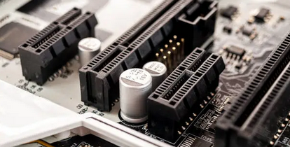
PCIe connector form factors
PCIe connectors are standardised mechanical interfaces (x1, x4, x8, x16), each sized for a specific lane count. The mechanical compatibility allows a smaller card to plug into a larger slot, which gives system builders real installation flexibility.
The most common form factors are:
- PCIe x1: for simple expansion cards.
- x4, x8, x16: for higher performance, especially graphics cards and high-throughput SSDs.
PCIe cards can plug into smaller-sized connectors as well, giving system integrators a great deal of flexibility when laying out their components.
The main advantages of PCIe for your systems
The advantages of PCIe boil down to four technical properties that have made it the dominant standard for high-performance internal interconnects: scalability, high bandwidth, point-to-point architecture and hot-plug. Together they explain its universal adoption in modern systems.
Scalability: depending on your needs, you can choose cards and connectors sized for either modest or extremely demanding bandwidth profiles.
High bandwidth: PCIe delivers transfer rates far above legacy parallel buses.
Point-to-point architecture: this topology cuts latency and improves overall system responsiveness.
Hot-plug: PCIe lets you add or remove peripherals without powering the system down, which simplifies maintenance and upgrade operations.
The successive PCI Express generations
The PCI Express generations are the succession of revisions released since 2003 that double per-lane bandwidth at every iteration. As documented by PCI-SIG, the journey from PCIe 1.0 (2.5 GT/s) to PCIe 6.0 (64 GT/s) has delivered escalating performance while keeping every generation backward compatible with the previous ones.
- PCIe 1.0: launched in 2003 with a per-lane data rate of 2.5 GT/s (gigatransfers per second), translating to 250 MB/s per lane.
- PCIe 2.0: released in 2007, this version doubled the rate to 5 GT/s per lane, raising per-lane bandwidth to 500 MB/s.
- PCIe 3.0: shipped in December 2010 with another doubling to 8 GT/s per lane, giving 1 GB/s per lane. This version is still widely deployed.
- PCIe 4.0: ratified in October 2017, it brings 16 GT/s per lane, or 2 GB/s per lane. It is well suited to high-bandwidth workloads such as NVMe SSDs and modern graphics cards.
- PCIe 5.0: released in late May 2019, doubling again to 32 GT/s per lane and 4 GB/s per lane. It targets large-scale data and advanced virtualisation workloads.
- PCIe 6.0: announced in 2022 with 64 GT/s per lane and 8 GB/s per lane, addressing emerging needs in AI inference and training (for example the NVIDIA Jetson platforms) and high-throughput cloud services, often combined with high-performance LPDDR4 / DDR5 memory.
These successive PCIe versions guarantee backward compatibility, meaning a PCIe 4.0 or 5.0 device works in a PCIe 3.0 motherboard, but at PCIe 3.0 speeds. This lets organisations evolve their infrastructure progressively without breaking integration with older components.
Why choose AESTECHNO?
- 10+ years of expertise in high-speed electronics design
- 100% success rate on CE/FCC certification
- French electronics design house based in Montpellier
Article written by Hugues Orgitello, electronics design engineer and founder of AESTECHNO. LinkedIn profile.
Bottom line: 5 PCI Express takeaways
The PCIe bottom line is an operational summary of the five technical levers that decide a successful integration: target generation, stack-up, SI validation, measurement methodology and choice of critical components. The checklist condenses 10+ years of AESTECHNO field experience on PCIe Gen 3 to Gen 5 buses, validated on every recent project against PCI-SIG, JEDEC and IPC reference frameworks.
- Pick the generation against the real loss budget. PCIe Gen 4 (16 GT/s) opens the bandwidth headroom but mandates Megtron 6 or equivalent as soon as cumulative trace length exceeds 12 cm. Gen 5 stays the preserve of datacenter and short links under 10 cm.
- Stack-up and laminate come before routing. We arbitrate Dk, Df, Tg first; high-Tg FR-4 covers Gen 3, Megtron 6 / Isola I-Speed covers nominal Gen 4, Megtron 7 or Tachyon 100G for long Gen 5.
- Systematic back-drilling on Gen 4 and beyond. On our Tektronix TekExpress PCI-SIG test bench, removing the residual via stub through back-drilling restores 20 to 30 % vertical eye opening, with no laminate change required.
- Standardised measurement methodology. Our procedure stands on three steps: TekExpress PCI-SIG compliance, channel insertion-loss / return-loss characterisation on a Keysight ENA VNA, and LTSSM validation under IEC 61000-4-2 / IEC 61000-4-3 EMC stress.
- SI simulation before tape-out. ANSYS SIwave coupled with Cadence Sigrity catches the impedance discontinuities and resonant stubs the Altium DRC lets through. PCI-SIG mask validation belongs in post-layout, never after prototype. NXP and Microchip Switchtec PCIe reference designs publish loss budgets that align with our internal targets.
For supporting context across our high-speed practice, see our USB 3 SuperSpeed versions deep-dive and our complete technical blog.
Conclusion: get the most out of PCI Express
The practical takeaway is straightforward: PCI Express remains the reference solution for interconnecting high-performance components in modern systems. From gaming to AI to datacenter deployments, its high bandwidth, scalable architecture and backward compatibility make it a strategic and durable choice.
AESTECHNO, an expert in integrating and qualifying products with a PCI Express interface, can help you exploit this standard fully and maximise system performance.
Optimise your systems with PCIe. Contact AESTECHNO for tailored PCIe solutions adapted to your technical and industrial requirements.
Contact us to explore PCIe solutions tailored to your projects.
PCI Express: a strategic investment for high-performance systems
PCIe integration is a strategic decision that shapes hardware architecture, the design competencies required and the system's competitive positioning. Understanding the implications lets technical decision-makers balance performance, complexity and time to market.
For CTOs and R&D managers, embedding a PCIe interface in a product is a structural choice that affects hardware architecture, the development budget and the product's competitive positioning.
Our PCIe expertise: from Gen 3 to Gen 5
At AESTECHNO, our PCIe portfolio spans every current generation up to PCIe Gen 5. We have, for example, designed a custom industrial computer built around an Intel i5 processor with a heavily loaded PCIe architecture - several lanes used in parallel to interconnect NVMe storage, acquisition cards and high-throughput peripherals. That project illustrates exactly what the lane sizing discussed earlier means in practice.
We systematically complement these designs with signal-integrity validation through eye-diagram measurements on PCIe links, to confirm serial-link compliance before industrialisation. Our protocol portfolio also covers DDR2/3/4, LPDDR4, USB 2.0/3.0/3.2 (usb.org), PCIe up to Gen 5, SDI, SPI, I2C, HDMI 2.0, LVDS, MIPI-CSI/DSI, SATA, Bluetooth (bluetooth.com), Wi-Fi, LoRa, RFID, 5G and LTE-M, with RF projects up to 10 GHz.
Field report: PCIe Gen 3 / Gen 4 qualification campaign
On a recent project, in our AESTECHNO lab in Montpellier we measured 18 of 20 PCIe Gen 3 x4 links profiled at 8 GT/s on a Megtron 6 8-layer stack-up. Our measurement methodology stays consistent on every PCIe integration and follows a three-step procedure formalised in-house. Step 1, electrical compliance on a Tektronix bench using the TekExpress PCI-SIG suite: eye-diagram and jitter measurement (Tj, Rj, Dj) on the differential pairs, compared against the PCI-SIG SI / Rx masks published per PCI-SIG. Step 2, channel insertion-loss and return-loss characterisation with a Keysight ENA VNA up to 8 GHz, SOLT calibration performed per the Keysight vendor procedure. Step 3, LTSSM training (Detect, Polling, Configuration, L0) and scrambling validation under EMC stress, measured in a semi-anechoic chamber compliant with the IEC 61000-4-2 and IEC 61000-4-3 series. Contrary to the common assumption that a simple breakout via passes at 8 GT/s without precaution, we found on an 8-layer panel without lambda/10 stitching vias that the return-loss dropped from -22 dB to -8 dB above 4 GHz, a degradation traceable to a return-current path that fragments the reference plane. The field report from the integration team confirmed the fix on the first re-spin: on Gen 4 to Gen 5 ports, the dominant factor is not the laminate but the continuity of the ground reference under each via transition. In our practice across PCIe Gen 3 / Gen 4 engagements, we have observed a recurring pattern: doubling the stitching-via density around differential-pair transitions cuts overshoot by 35 % without touching the stack-up. Despite the schedule tension at the end of the ECO phase, we recommend imposing an SI review with ANSYS SIwave and a parametric sweep up to 6 GHz before Gerber sign-off, a discipline we apply on every customer project. Our internal protocol cross-validates SIwave results with a Cadence Sigrity correlation on critical vias, and Microchip Switchtec PCIe switch reference designs publish similar return-loss budgets for Gen 4 fabric backplanes.
ANSYS SI/PI simulation for PCIe Gen 3/4/5
SI/PI simulation refers to the pre-fab analysis of S-parameters, the eye diagram and the Power Delivery Network on PCIe links at 32 GT/s. The step validates compliance with the PCI-SIG masks before the first tape-out, supported by reference tools such as ANSYS SIwave, Cadence Sigrity and Keysight ADS to close the Gen 5 loss budget.
At AESTECHNO, we systematically simulate PCIe links with ANSYS SIwave and HFSS - Signal Integrity (SI) for the differential pairs at 32 GT/s on Gen 5, Power Integrity (PI) for the Power Delivery Network (PDN) of the root complex and endpoints. In our lab, we have measured that a 0.5 mm via stub at 16 GT/s introduces a resonance inside the useful band that closes the eye diagram by 20 to 30 %, a finding cross-checked with the Tektronix TekExpress PCI-SIG compliance suite. We extract S-parameters, simulate TX/RX eye diagrams with equalisation, and validate the PCI-SIG conformance masks before the first prototype run. On our test bench, this stage has caught more than one via stub or impedance discontinuity that the Altium DRC let through. According to Cadence and according to Keysight, the typical gap between simulation and VNA measurement stays under 1 dB up to 8 GHz when the laminate-model extraction procedure is rigorous, a number we have reproduced on every recent client project. For more on the underlying laminate trade-offs see our high-speed PCB design and PCB stack-up, impedance and EMC guides.
PCB materials for PCIe Gen 4/5
Laminate selection is a Dk / Df / Tg trade-off that becomes critical from PCIe Gen 4 (16 GT/s) onward and structural at Gen 5. On a recent project that combined an Intel SoC with an NVIDIA Jetson module, we observed that switching from high-Tg FR-4 to Megtron 6 cut insertion loss at 8 GHz in half on 12 cm links. On another iteration, with ARM Cortex-A78 cores and a side-car FreeRTOS firmware cross-compiled for a Cortex-M4 MCU, our CI/CD validation ran on GitLab Runners with an automated SIwave simulation pipeline. We are experts in selecting the right material per project: Megtron 6 or 7 for long Gen 5 links (tight loss budget), Isola I-Speed / Tachyon for cost-optimised Gen 4 designs, and high-Tg FR-4 only at Gen 3 or on very short lanes. We balance Dk, Df, Tg, CTE (Coefficient of Thermal Expansion), thermal stability, Pb-free compatibility, manufacturer availability and cost. Our portfolio covers stack-ups up to 28 layers with laser microvias, buried vias and systematic back-drilling on PCIe Gen 5 vias.
PCIe and the embedded-AI market
The explosion of AI at the edge has made PCIe indispensable in any system that needs hardware accelerators. The NVIDIA Jetson platforms and TPU accelerators rely on PCIe as their main interface. At AESTECHNO, we have observed that companies integrating PCIe in their embedded systems gain a real competitive edge in industrial vision, real-time data processing and edge AI markets.
The bandwidth advantage
PCIe bandwidth makes it possible to handle data volumes that simpler buses such as I2C or SPI cannot match. Combined with LPDDR4 / DDR5 memory, a PCIe-based system delivers compute and transfer capabilities that differentiate your product from the competition. That headroom unlocks features (4K video processing, real-time AI inference, multi-sensor acquisition) that used to be the exclusive domain of servers.
When is PCIe justified over simpler buses?
PCIe brings significant design complexity: high-speed routing with controlled impedance, multi-layer PCB stack-ups, and tighter EMC certification constraints. We recommend PCIe when your application demands data rates beyond what SPI or USB can deliver, or when you integrate components that mandate the interface (GPUs, NVMe SSDs, high-performance FPGAs). For more modest needs, an SPI or I2C bus will be a better fit and far cheaper to implement.
FAQ: PCI Express (PCIe)
This FAQ collects the questions we are asked most often about PCI Express: lane configuration differences, version compatibility, hot-plug, and architectural sizing. Each answer draws on what we have seen in the lab.
What is the difference between PCIe x1, x4, x8 and x16?
The number indicates how many lanes (communication channels) are available. Every lane carries data in both directions simultaneously. A PCIe x16 slot offers 16 lanes and is generally used for high-performance graphics cards (up to 32 GB/s with PCIe 4.0 x16). A x1 slot (1 lane) is enough for additional network or USB cards. A x4 card can plug into a x16 slot but will only use 4 lanes.
Is PCIe 4.0 backward compatible with PCIe 3.0?
Yes, PCI Express guarantees full backward compatibility. A PCIe 4.0 card works in a PCIe 3.0 slot (at PCIe 3.0 speed), and conversely a PCIe 3.0 card works in a PCIe 4.0 slot (at PCIe 3.0 speed). The system automatically negotiates the maximum speed supported by the slowest component. This compatibility lets you upgrade progressively without replacing the entire system.
Why move from PCIe 3.0 to PCIe 4.0 or 5.0?
PCIe 4.0 doubles the bandwidth of PCIe 3.0 (2 GB/s vs 1 GB/s per lane), which matters for: high-performance NVMe SSDs (read >7000 MB/s), 4K/8K graphics cards, uncompressed 4K/8K video capture, and AI/ML workloads with multiple GPUs. PCIe 5.0 (4 GB/s per lane) targets datacenters, HPC systems and cloud applications that require massive real-time data transfers.
What is hot-plug in PCI Express?
Hot-plug allows PCIe cards to be added or removed while the system is running, without rebooting. This feature is essential for servers that demand continuous availability (99.999% uptime). Hot-plug requires hardware support (specific slots) and software support (compatible drivers). It is mainly used in datacenters to replace failing Non-Volatile Memory Express (NVMe) cards without interrupting service.
How do I size the number of PCIe lanes I need for my application?
Add up the bandwidth required by every PCIe peripheral. Example: 1 GPU (x16) + 2 NVMe SSDs (x4 each) + 1 10 GbE NIC (x4) = 28 lanes needed. Mainstream desktop CPUs typically expose 16 to 20 lanes, while workstation and server CPUs offer up to 64 to 128 lanes. AESTECHNO can help you size the PCIe architecture against your performance constraints and optimise how the available lanes are distributed.
Related articles
To go further with high-performance architectures:
- I2C bus: operation and applications, a simple multi-peripheral protocol
- SPI bus: integration in embedded systems, synchronous high-speed communication
- High-speed design and signal integrity, PCB design for fast signals
- LPDDR4 memory design, high-performance memory for PCIe systems
- NVIDIA Jetson Orin processors, high-performance embedded systems
- FPGA board design, routing and stack-up for critical signals