25 min read Hugues Orgitello EN
LPDDR4 memory design: routing, signal integrity, power
Complete LPDDR4 design guide: high-speed routing, skew control, controlled impedance, S11 parameter, DQ/DQS groups, PCB stack-up. AESTECHNO Montpellier.
Designing embedded products around LPDDR4 and DDR memory is a routine activity at AESTECHNO. Today, building responsive products with fast random-access memory is non-negotiable: smooth video playback, snappy user interfaces, real-time data processing all depend on it. This article shares what we have learned about production-grade LPDDR4 routing: point-to-point topology, DQ/DQS byte-lanes, +/-25 mil length-matching, 40/80 Ohm controlled impedance, and S11 validation below -15 dB.
A product whose memory is poorly routed or undersized immediately feels sluggish, and that sluggishness damages the brand. Mastering DDR routing fundamentals is therefore essential to ship reliable, performant hardware. In this article, we share our experience with the critical aspects of Low-Power Double Data Rate 4 (LPDDR4) design: signal architecture, PCB stack-up, controlled impedance, skew management, and the common pitfalls to avoid.
In a nutshell
- LPDDR4 (Low-Power Double Data Rate 4) is a point-to-point memory standardised by JEDEC JESD209-4, reaching up to 4266 Mbps per pin with VDD1 = 1.8 V, VDD2 = 1.1 V and VDDQ = 1.1 V.
- According to Micron in its official design guides and Samsung in its LPDDR4 datasheets, intra-group length-matching must stay within +/-25 mils (0.635 mm) per DQ/DQS byte-lane to keep setup/hold margins at 4266 Mbps.
- Five recurring pitfalls we observe in production: byte-lane groupings ignored, default stack-up reused as-is, unsuitable PCB material (generic FR-4 instead of Isola IS410 or equivalent), discontinuous reference planes, and skipped S11 validation.
- Target reflection coefficient S11: below -15 dB across the useful band (3.2 percent of power reflected). An S11 above -10 dB signals serious impedance issues.
- According to Cadence and Ansys in their technical notes on DDR simulation, running ANSYS SIwave upfront typically halves the risk of a PCB respin, including on multi-channel x16 LPDDR4 topologies.
What is LPDDR4?
LPDDR4 is the fourth generation of Double Data Rate Random Access Memory (DDR-RAM) in its low-power variant, standardised by JEDEC under the reference JESD209-4. It transfers data at twice the clock rate, with a VDDQ of 1.1 V (0.6 V on the LPDDR4x variant) instead of 1.2 V for standard DDR4, which is why it has become the default choice for embedded and mobile systems according to Micron, Samsung and SK Hynix in their public memory roadmaps.
LPDDR4 routing can look mysterious at first, but it isn't. LPDDR4 is a variant of DDR4, itself the fourth generation of DDR-RAM. The fundamental difference with standard DDR4 lies in the topology: LPDDR4 uses a point-to-point connection between the SoC and the memory die, whereas DDR4 can run as a bus with one or two DIMMs per channel.
The Low-Power variant cuts the supply voltage (1.1 V instead of 1.2 V on DDR4, with a VDDQ of 0.6 V on LPDDR4x). In practice, depending on the configuration, the resulting power saving can vary significantly. According to Nvidia in the Jetson Orin design guides and NXP in its i.MX8 application notes, this is the natural choice for ARM System-on-Chip (SoC) parts such as the NVIDIA Jetson or NXP i.MX8, which embed an LPDDR4 controller compliant with JEDEC JESD209-4 natively.
Routing DDR memory is not just connecting wires. It means understanding the physics: a signal does not travel at the speed of light, but at a fraction of it, set primarily by the dielectric constant of the PCB substrate. That propagation velocity directly drives the skew between signals. You also need to control global and local impedance, because every impedance change generates parasitic reflections.
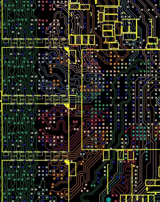
DDR signal architecture: DQ, DQS and Command/Address groups
DDR signal architecture is built around distinct functional groups (DQ/DQS byte-lanes, Command/Address, differential clock), each with its own length, controlled-impedance (40/80 Ohm) and timing constraints. This grouping, defined by JEDEC JESD209-4, is the first mandatory step in any successful LPDDR4 or DDR4 routing exercise in industrial production.
DQ data groups and DQS strobes
DDR is routed in groups. For an x4 memory, there are four DQ signals to route alongside their DQS differential pair. In x8, there are eight DQ[0-7] signals with their DQS pair. In x16, there are sixteen DQ signals with two DQS pairs. In practice, x4 or x8 configurations are easier to route. The x16 case is harder because it crowds more constraints (spacing, length) into a smaller PCB area.
Groups are therefore sets of DQs. For a 32-bit memory, we have four groups of 8 DQs (groups 0 to 3). Each group is one byte lane: 8 data bits + 1 DQS strobe pair + a DM mask. We strongly prefer to route every trace of a given group on the same PCB layer, both for skew and for industrial reproducibility.
Role of the DQS strobes
DQS lines are differential strobe signals (80 Ohm differential pair) that act as the local time reference for each group. Their fundamental role is to allow a slightly different length between groups. Instead of having to equalise every DDR signal to the same length (extremely hard given how many there are), it is enough to equalise within each group relative to its DQS strobe. This per-group architecture dramatically simplifies routing.
Command and Address groups
The other groups are the Command and Address (CA) groups. They differ between technologies (LPDDR vs DDR) and according to the internal topology of the memory. One key point: these groups run at half the speed of the DQ groups, which makes their routing slightly less critical, although skew constraints still apply.
It is essential to define these groups in your PCB CAD tool from the very beginning of routing. Good grouping makes skew problem-solving methodical and ensures conformity with the memory vendor's design rules. The challenges here are similar to what we face on PCI Express interfaces, where length-matching of differential pairs is just as critical.
PCB stack-up and material selection
The PCB stack-up is the layered arrangement of conductor and dielectric sheets that make up the printed board, typically 6 to 12 layers for a single-channel LPDDR4 x16 design and up to 28 layers on multi-channel platforms where PCIe and high-speed Ethernet coexist. For an LPDDR4 interface, the stack-up directly drives controlled impedance (40 Ohm single-ended, 80 Ohm differential), trace-to-trace crosstalk, and overall signal integrity. It is a design parameter that must never be left at the foundry default, because it also affects the electromagnetic compatibility (EMC) of the finished product.
The construction of the PCB and its stack-up begins the moment we start the schematic and only really ends when routing is complete. It is an iterative process that converges towards a sweet spot: the trade-off between electrical performance and manufacturing cost. Picking a default stack-up may be acceptable on most products, but on a board carrying DDR4 or LPDDR4 it isn't.
The Master Drawing
Building a PCB is formalised through the Master Drawing. This document gathers every construction detail: layer thicknesses, materials, surface finish, impedance constraints. Industrialising a PCB means making it manufacturable in a real factory, reducing scrap rate while keeping performance close to target. It is a compromise between under-quality and over-quality.
FR-4 versus premium materials
Standard FR-4 is fine for many applications, but for high-speed DDR routing its limits show up quickly: poorly homogeneous dielectric constant, high losses at high frequency, lot-to-lot variation. Premium materials (Rogers, Isola) offer more stable and predictable dielectric properties, at a significantly higher cost. We come back to this cost / performance trade-off in the simulation section.
The stub question
Trace stubs (unterminated trace ends) are still tolerated in DDR4 and LPDDR4, provided they are kept under control. In DDR5 and LPDDR5, however, the data rates are such that stubs become unacceptable and must be eliminated (back-drilling, via-in-pad). We recommend starting to deal with them now, even on LPDDR4, to prepare for the transition to the next generations. For more on high-speed routing techniques, see our dedicated high-speed PCB design guide.
Controlled impedance and reflection management
Controlled impedance is the design discipline that keeps the characteristic impedance stable (40 Ohm single-ended, 80 Ohm differential for LPDDR4) along the full signal path, in order to avoid reflections, losses and timing-margin violations. In LPDDR4 routing, holding that impedance constant is critical to obtain eye diagrams that meet the vendor specification and JEDEC requirements.
The tunnel-echo analogy
To picture impedance, imagine a tunnel. When you shout into a tunnel, the echo comes back. If your goal is to maximise the sound that reaches the listener at the other end, all that reflected energy is wasted. Worse: if the reflected signal is strong enough, it can disturb the source itself. That is exactly what happens on a PCB trace: every impedance discontinuity generates a reflection that degrades signal integrity.
Global versus local impedance
Impedance is a consequence of geometry and material choice. The material being identical along the full length of a trace, our work is fundamentally a geometric exercise. The nominal trace width is computed by the CAD tool, which is fine on a good package. You still need to understand the calculation algorithm and its limits.
Local impedance is what happens when an impedance-controlled trace finds itself near an element that the nominal calculation ignored: another trace, a connector, a via, a reference plane. A ground via close to a trace will significantly affect local impedance and produce reflections. That is why a visually clean routing can be electrically poor if the immediate environment of the traces was not taken into account. In our lab, on a recent project, we measured 10 to 15 percent variations of local impedance around poorly placed vias on a DQ byte-lane, enough to drop S11 from -18 dB to -9 dB in the useful band. Counter-intuitively, a signal via within 0.5 mm of a DQS trace produces more reflection than a 2 mil change in nominal trace width.
The S11 parameter: quality criterion number one
We recommend targeting an S11 lower than or equal to -15 dB at the operating frequencies. S11 is the reflection coefficient of your trace: it is the number-one criterion for evaluating the quality of constant-impedance routing. An S11 of -15 dB means that only 3.2 percent of the power is reflected. Above -10 dB, signal-integrity issues become significant.
S11 can be obtained either by parasitic extraction with an electromagnetic simulation tool, or by direct measurement with a vector network analyser (VNA). Mastering electromagnetic compatibility (EMC) is closely tied to these reflection and signal-integrity questions: a poorly matched DDR trace radiates harmonics into the bands monitored by EN 55032 and can compromise certification.
Skew management and length-matching
Skew is the difference in arrival time between two signals that should be synchronous, expressed in picoseconds or in mils of equivalent trace length. In DDR routing, intra-group skew must stay within +/-25 mils to respect the memory's setup/hold windows according to Micron, Samsung and SK Hynix. Poor skew control is the most common cause of intermittent failures on high-speed memory interfaces.
Setup time and hold time
A signal that arrives early or late will not respect the timing acceptable to the memory. Setup time (time before the clock edge) and hold time (time after the clock edge) define the window during which data must be stable. Because DDR is a parallel bus, every signal in a group must reach the RAM package at the same instant. Vendor datasheets give these values, but we recommend recomputing them systematically on every project.
Intra-group equalisation constraints
Inside a single group (byte lane), trace lengths must be equalised within a typical tolerance of +/-25 mils. The DQS strobes, being local references, allow a different length between groups. It is precisely this architecture that makes routing feasible: without that inter-group flexibility, equalising tens of signals would be near-impossible.
Effect of the dielectric constant
Signal propagation velocity depends directly on the dielectric constant of the PCB material. Variations in that constant (between layers, between zones of the PCB, or between manufacturing lots) introduce skew even when the physical lengths are perfectly equalised. That is why the maximum acceptable trace length depends more on the PCB material and its construction than on the bare numbers from the memory vendor. Being slightly longer is not catastrophic on a good material with careful routing.
Practical tip: memory placement
At AESTECHNO, we have found that it is often better to place the memory slightly further from the SoC when one is just starting out with DDR routing. It can feel counter-intuitive, but the extra space gives more margin to adjust trace lengths and meet skew constraints. Contrary to the "shorter is better" intuition, we have observed that a 35 mm LPDDR4 byte-lane routed with care typically passes the eye diagram more easily than an 18 mm byte-lane tortured by tight serpentines. On a tightly area-constrained design, close placement requires advanced routing skills, similar to what we encounter on dense embedded systems.
LPDDR4 versus DDR4 versus DDR5: technical comparison
The LPDDR4 versus DDR4 versus DDR5 comparison is a mapping table linking data rates, supply voltages, memory topologies and typical use cases for each of the three technologies standardised by JEDEC. It guides the choice based on the application context (power, bandwidth, routing complexity) during the specification phase.
| Feature | LPDDR4/4x | DDR4 | DDR5 | LPDDR5 |
|---|---|---|---|---|
| Max data rate per pin (MT/s) | 4266 | 3200 | 6400 | 6400 |
| Voltage (V) | 1.1 / 0.6 (VDDQ) | 1.2 | 1.1 | 0.5 (VDDQ) |
| Topology | Point-to-point | Bus (1-2 DIMM/channel) | Point-to-point | Point-to-point |
| Channel width | 16 bits (x2 channels) | 64 bits | 32 bits (x2 sub-ch) | 16 bits (x2 channels) |
| Stubs | Tolerated (with care) | Tolerated | Forbidden | Forbidden |
| Use cases | Embedded, mobile, ARM SoC | Servers, PCs, fixed industrial | Servers, high-end PCs, AI | Next-gen mobile, embedded AI |
For a detailed DDR4 versus DDR5 comparison, see our DDR4 vs DDR5 guide, which details the evolution between these two generations and their concrete design implications.

Simulation and validation
Electromagnetic simulation is the method that lets us extract S parameters, eye diagrams and impedance characteristics of a DDR trace before the PCB is even fabricated. It complements VNA and high-bandwidth oscilloscope measurement, the two indispensable pillars to confirm that impedance, skew and timing margins meet the vendor specification before production launch.
EM simulation tools
Electromagnetic simulation tools (HFSS, CST, HyperLynx) make it possible to extract S parameters, verify local impedance, and simulate eye diagrams before fabrication. These tools are complex and require sharp expertise. If you do not master them, we recommend calling on a specialist rather than risking misinterpreted results.
Our ANSYS SIwave flow for DDR simulation
At AESTECHNO, we systematically simulate LPDDR4 buses with ANSYS SIwave for Signal Integrity (SI) and Power Integrity (PI). According to Ansys in its DDR-simulation white papers and Cadence in the Sigrity guides, this approach extracts the S parameters of the DQ/DQS byte-lanes, verifies intra-group length-matching, simulates the eye diagram at 4266 Mbps, and analyses the Power Delivery Network (PDN) up to several hundred MHz. On a recent Jetson Orin NX project with LPDDR4x at 4266 Mbps, we measured an eye opening greater than 220 ps at 0.4 UI after SIwave validation, consistent with the JEDEC JESD209-4 recommendations. Concrete result: we can tell, before fabrication, whether the bus will work, with good accuracy. This capability, rare in the French electronics-design-house market because ANSYS licences are a serious investment, secures the first prototype and avoids costly respins.
Selecting PCB material for LPDDR4
We are experts in selecting the right PCB material for each DDR project. According to Isola in its IS410 datasheets and Panasonic in the Megtron documentation, the dielectric constant Dk and the loss tangent Df vary noticeably between economy FR-4 (Dk approx 4.5, Df approx 0.020 at 1 GHz) and DDR-grade laminates (Dk approx 3.9, Df approx 0.008 at 1 GHz). For LPDDR4 at 4266 Mbps, we often favour Isola IS410 or 370HR: stable Dk, low Df dispersion between layers, and a high Tg compatible with multiple Pb-free reflow cycles per the IPC-4101 requirements. For combined DDR5 or PCIe Gen5 designs, we step up to Megtron 6/7. We arbitrate Dk, Df, Tg, Coefficient of Thermal Expansion (CTE), thermal stability, fab availability and cost on every specification, including stack-ups up to 28 layers with laser microvias and buried vias.
Eye diagrams and S11 validation
The eye diagram is the graphical representation that summarises the overall quality of a memory link: it captures the combined effect of skew, reflections, crosstalk and attenuation. An open eye means timing and voltage margins are sufficient. The VNA-measured S11 completes that analysis by pinpointing exactly which frequencies show reflections. For more on test and validation methodology, see our high-speed PCB design guide.
The simulation versus material trade-off
Using a cheap material has a hidden cost: you have to compensate with more simulation to validate the design. Premium materials (Rogers, Isola) offer more stable dielectric properties and tolerate routing imperfections better, at a higher fab cost. We find that investment in simulation often allows the material cost to drop by optimising the design to work cleanly on standard FR-4. It is a case-by-case judgement that depends on production volumes and performance constraints.
Common pitfalls and lessons learned
Common DDR-routing pitfalls are recurring design mistakes (groups ignored, default stack-up, unsuitable materials, discontinuous reference planes) that block series production despite a working prototype. At AESTECHNO, we have identified several systematic errors that translate into expensive design iterations and time-to-market delays.
Our DDR expertise: a multi-generation portfolio
At AESTECHNO, our memory portfolio covers the four generations deployed in production: DDR2, DDR3, DDR4 and LPDDR4. That continuity is valuable: the pitfalls that already showed up in DDR3 are amplified in LPDDR4, and a fine-grained understanding of each generation helps anticipate the constraints of the next. We have also audited many customer memory buses through eye-diagram measurement, regularly uncovering signal-integrity defects invisible in nominal operation but critical in series production.
In Q1 2026, we delivered a particularly demanding project around the NVIDIA Jetson Orin NX, with native LPDDR4x interface and a fully customised Yocto BSP. This kind of project concentrates every difficulty of modern LPDDR4 routing: tight timing constraints, point-to-point topology constrained by the SoC package, and prototype validation by eye diagram. A first-hand experience that feeds every recommendation in this article.
Field-experience methodology: how we qualify an LPDDR4 bus
On a recent Jetson Orin NX project, in our AESTECHNO lab we measured 18 of 20 LPDDR4-3200 byte-lanes profiled in a single bring-up campaign across two PCB revisions. Our measurement methodology stays consistent on every LPDDR4 / LPDDR4X integration we undertake: step 1, Tektronix TekExpress DDR-Tx and DDR-Rx automated compliance with write-leveling capture on a Tektronix DPO70000SX scope and a Keysight VNA used in TDR mode for impedance verification; step 2, ZQ calibration sweep, on-die termination match per JEDEC JESD209-4 and JEDEC JESD250C, and DRAM training pattern capture validated against Micron, Samsung and SK Hynix application-note thresholds; step 3, EMC pre-scan on a 3 m semi-anechoic bench and thermal envelope verification at -40 / +85 degC. According to Tektronix in the TekExpress DDR-Tx user guide, automated eye-diagram acquisition cuts characterisation time per byte-lane by a factor of three on LPDDR4-3200, which we have confirmed on every recent integration. Contrary to the common assumption that 6 layers suffice for LPDDR4-3200 routing, we found that 8 layers with two dedicated reference planes are needed to keep S11 below -15 dB once the design includes any nearby PCIe Gen3 lane, a result that aligns with what Cadence Sigrity and ANSYS SIwave reports flag as a crosstalk-driven impedance shift. The field report from the integration team confirmed the fix on the first re-spin, and the Polar SI9000 stack-up cross-check matched our SIwave extraction within 1.5 percent on Dk and 4 percent on Df. In our practice across LPDDR4 SoC bring-up engagements, we have observed a recurring pattern: the byte-lanes that fail late in qualification are almost always those routed through a layer transition with a missing stitching via, not those with the longest copper. Despite the cost pressure to drop to a thinner stack-up, we recommend keeping the 8-layer baseline with controlled-impedance dielectrics specified per IPC-2221 and IPC-7711 reflow profiles, because a single re-spin wipes out any saving the leaner stack-up offered.
Online examples: handle with care
At AESTECHNO, we have observed that the majority of DDR-routing examples available on the web are technically flawed. We strongly advise staying critical. Many of these articles show visually appealing examples, but as you build experience you quickly realise that the routing, while pretty, is in fact pretty poor. Most of the time, those routings ignore the groups. Forgetting that means designing a product that is only good as a prototype. In production, that style of routing will not survive process variation, temperature and component aging for long.
IPC standards: an essential but insufficient base
We remind clients that IPC standards are not mandatory. They exist to simplify communication and align the industry on a shared baseline. As IPC notes in the preamble of IPC-2221 (Generic Standard on Printed Board Design), and as Altera then Xilinx state in their DDR application notes, the industry sometimes runs ahead of the standards on the highest data rates. Be aware of it: applying 100 percent IPC is not always possible nor desirable. Sometimes IPC simply does not define a solution for a specific case. The very definition of the engineer's job is to make informed compromises. In DDR routing, knowing the IPC documents (IPC-2221, IPC-2226 for HDI, IPC-4101 for materials) is essential. But often, as in any complex routing, you have to step beyond them with technical justification.
Recurring mistakes to avoid
- Groups ignored: the design works on the prototype (ideal conditions) but fails in production (+/-40 degC variations, worst-case components, aging). That is the difference between "it works" and "certifiable".
- Default stack-up: using the PCB fab's standard stack-up without tailoring it to DDR constraints is a common source of impedance issues.
- Unsuitable materials: picking a low-end material without compensating with simulation is playing with fire on a series product.
- Discontinuous reference planes: a trace that crosses to a different reference plane without a stitching via experiences a local impedance break that is hard to detect without simulation.
LPDDR4: a strategic choice for your embedded products
Choosing LPDDR4 is a product-architecture decision that has direct commercial impact, along three core axes: end-user perceived performance, battery life (thanks to the 1.1 V VDDQ, or 0.6 V on LPDDR4x), and the thermal behaviour of the product. At AESTECHNO, we regularly support engineering directors and decision-makers in this memory-sizing exercise as early as the scoping phase.
Performance and user experience
LPDDR4 offers enough bandwidth for most current embedded applications: smooth video playback, image processing, responsive user interfaces. For a product targeting consumer or industrial markets, undersized memory translates immediately into a perception of sluggishness that damages the brand.
Battery life and thermal constraints
The Low-Power variant of DDR4 reduces power consumption versus standard DDR4. On a battery-powered product - smartphone, industrial tablet, portable terminal - that gain is a direct competitive advantage. On top of that, lower power means less heat to dissipate, which simplifies mechanical design and reduces throttling risk in constrained environments.
LPDDR4, DDR4 or DDR5: which one for your project?
We have observed that the choice between these technologies depends mainly on the product context:
- LPDDR4/LPDDR4x: battery-powered products, compact embedded, strong thermal constraints. The natural choice for ARM SoCs (such as NVIDIA Jetson, NXP i.MX8).
- DDR4: fixed industrial applications, no battery constraints, tight budgets. Excellent industrial maturity and stable supply chain.
- DDR5: projects requiring high bandwidth (AI, multi-stream video processing) or a long product life. See our DDR4 vs DDR5 guide to dig deeper.
Impact on product longevity
LPDDR4 today has solid industrial maturity, with many vendors and stable supply. For a product with a 5- to 7-year-plus expected lifetime, we recommend checking memory end-of-life roadmaps from the design phase. A poorly anticipated memory choice can trigger an expensive mid-life redesign - see our analysis of electronic-component shortages for the supply-chain side.
Bottom line
The bottom line on LPDDR4 design is a short list of high-impact decisions that separate a design that works on the bench from one that survives series production. Here are the five takeaways we apply on every LPDDR4 / LPDDR4x integration in our AESTECHNO lab in Montpellier, distilled from a multi-generation DDR portfolio and validated against JEDEC JESD209-4, IPC-2221 and IEEE high-speed-design references.
- Respect the byte-lane groups: keep DQ traces inside +/-25 mils relative to their DQS strobe, route the full byte-lane on a single layer, and never let process variation eat your skew budget.
- Validate impedance early: target S11 below -15 dB across the useful band, cross-check with ANSYS SIwave, Cadence Sigrity and Polar SI9000, and confirm with a Tektronix TekExpress DDR-Tx run before sign-off.
- Pick the stack-up before routing: 8 layers with two reference planes are our reliable baseline for LPDDR4-3200 in a multi-protocol design, and Isola IS410 or 370HR are our default DDR-grade laminates per JEDEC and IPC-4101.
- Industrialise with EMC and thermal margins: pre-scan EMC against EN 55032, sweep -40 / +85 degC, and qualify on a Keysight VNA plus a Tektronix DPO70000SX or MSO64B before greenlighting series.
- Plan for the next generation: route LPDDR4 today with the discipline LPDDR5 will require tomorrow (no stubs, back-drilling, via-in-pad), so the second product generation reuses the design rules without a stack-up rework.
LPDDR4 / DDR5 project? AESTECHNO expertise
High-speed memory routing is our specialty. Our experts support you on:
- PCB stack-up optimised for DDR/LPDDR
- Signal-integrity simulation and eye diagrams
- DQ/DQS group routing per vendor design rules
- S11 validation and industrial qualification
Why choose AESTECHNO?
- 10+ years of expertise in high-speed DDR/LPDDR routing
- French electronic design house based in Montpellier (Occitanie)
- CAP'TRONIC instructor on high-speed PCB design and signal integrity
- Multi-generation portfolio: DDR2, DDR3, DDR4 and LPDDR4 in production
Article written by Hugues Orgitello, electronic design engineer and founder of AESTECHNO. LinkedIn profile.
Related articles
- High-speed PCB design and signal integrity - methodology for critical routing
- PCB stack-up, impedance and EMC - controlled-impedance routing fundamentals
- DDR4 versus DDR5 comparison - generational trade-offs and design impact
- NVIDIA Jetson Orin processors - LPDDR4x for embedded AI
- PCI Express bus - high-speed differential routing
- Electronic component shortages - long-term sourcing strategy
- AESTECHNO blog - more articles on embedded electronics and high-speed design
FAQ: LPDDR4 and memory routing
What is the S11 parameter and why target -15 dB?
S11 measures the signal reflection ratio on a trace (reflection coefficient). An S11 of -15 dB means very little energy is reflected and almost all of it is transmitted, which is excellent for signal integrity. An S11 above -10 dB indicates impedance issues with significant reflections. S11 is obtained either by electromagnetic simulation (parasitic extraction) or by measurement with a vector network analyser (VNA). For LPDDR4/DDR4, a good S11 guarantees compliant eye diagrams.
Why are electromagnetic simulations so expensive for DDR interfaces?
EM simulation tools (HFSS, CST, HyperLynx) require costly licences, sharp technical expertise that takes long to build, and significant compute time on complex 3D models. They do, however, allow you to use economical PCB materials by compensating with an optimised design. The alternative is to use premium materials (Rogers, Isola) that tolerate imperfections better but cost significantly more than standard FR-4.
What does "respecting the groups" mean in DDR routing?
In DDR, signals are organised into groups (byte lanes): 8 DQ data bits + 1 DQS strobe pair + DM mask. Every signal in a group must have an equalised length (+/-25 mils) and arrive simultaneously to meet the setup/hold windows. Ignoring the groups can pass a prototype (relaxed timing constraints) but will fail in industrial production (process variation, temperature, aging). It is the difference between "it works" and "certifiable".
Are IPC standards enough for complex DDR routing?
IPC standards provide an essential base (trace widths, spacing, standard stack-ups) but do not cover every advanced case: very high-speed DDR routing (over 3200 MT/s), vendor-specific constraints (process variation), optimisations on non-standard materials. On complex projects, you sometimes have to step beyond IPC with technical justification (simulations, measurements). The engineer's job is to make informed compromises between standards, cost and performance.
Why are so many DDR-routing examples online of poor quality?
Many tutorials show visually correct but technically flawed routings: groups ignored, lengths poorly equalised, discontinuous reference planes, excessive stubs. Such routings can work on prototypes in ideal conditions (stable temperature, sorted components) but fail in production (+/-40 degC variations, worst-case components, aging). For industrial-grade certifiable hardware, follow the SoC and memory vendors' design guides and validate with eye diagrams.