
High-reliability electronics design, from schematic to production-ready routing.
A PCB delivered by us is a PCB you can manufacture at scale, certify without rework, and assemble in the factory without surprises. EMC, IPC standards and DFM are built into the schematic, not added after the prototype smokes. Our hardware engineering services are contracted on the board we deliver, not on the hours we spend on it.
Expertise led by Hugues Orgitello, electronic-design engineer and founder of AESTECHNO Montpellier (10+ years of experience, certified CAP'TRONIC instructor).
- CE
- FCC
- ETSI EN 300 328
- IPC-A-610
- IPC-2221
Routing isn't a detail, it's the product
Most industrial projects that fail EMC certification don't suffer from a component defect, but from a routing defect. Perforated ground planes, poorly anticipated current return paths, misplaced decoupling: these errors don't show on the schematic, but they measure in the anechoic chamber.
At AESTECHNO, with over 10 years of experience, routing is treated as an engineering discipline in its own right. Our PCB hardware design engineer holds the IPC CID+ certification (Advanced Certified Interconnect Designer), a designer-level IPC credential covering fabrication materials, electrical and signalling issues and high-end design. We design pre-compliant CE/FCC boards, which means the first anechoic chamber test campaign is used to verify compliance, not to correct it. Our success rate: 100% on first pass. See our complete guide: PCB design secrets revealed.
High-frequency: MIPI, LPDDR4, PCIe, USB 3.x
Modern buses (MIPI CSI-2 at 4.5 Gbps, LPDDR4 at 4266 MT/s, PCIe Gen4 at 16 GT/s, PCIe Gen5) forgive no approximation: differential impedance control to ±5%, length equalization to the mil, rigorous anti-skew, eye diagram simulation before fabrication.
On a recent project integrating an i.MX 8 with LPDDR4, our routing achieved 4266 MT/s error-free on test bench at -20°C / +85°C, first try. This discipline is learned, and we have it. We have designed PCBs up to 28 layers, with laser micro-vias and buried vias for HDI applications. See our articles: PCI Express, LPDDR4 memory design, DDR4 vs DDR5.
Simulation before fabrication: the verdict before etching
We regularly use ANSYS simulation tools in-house, including SIwave and HFSS: high-speed digital simulation (eye diagram, jitter, inter-symbol interference), signal integrity (SI), power integrity (PI) and AI-assisted antenna optimization. The result fits in one sentence: we can tell before fabrication whether it's going to work, with good accuracy.
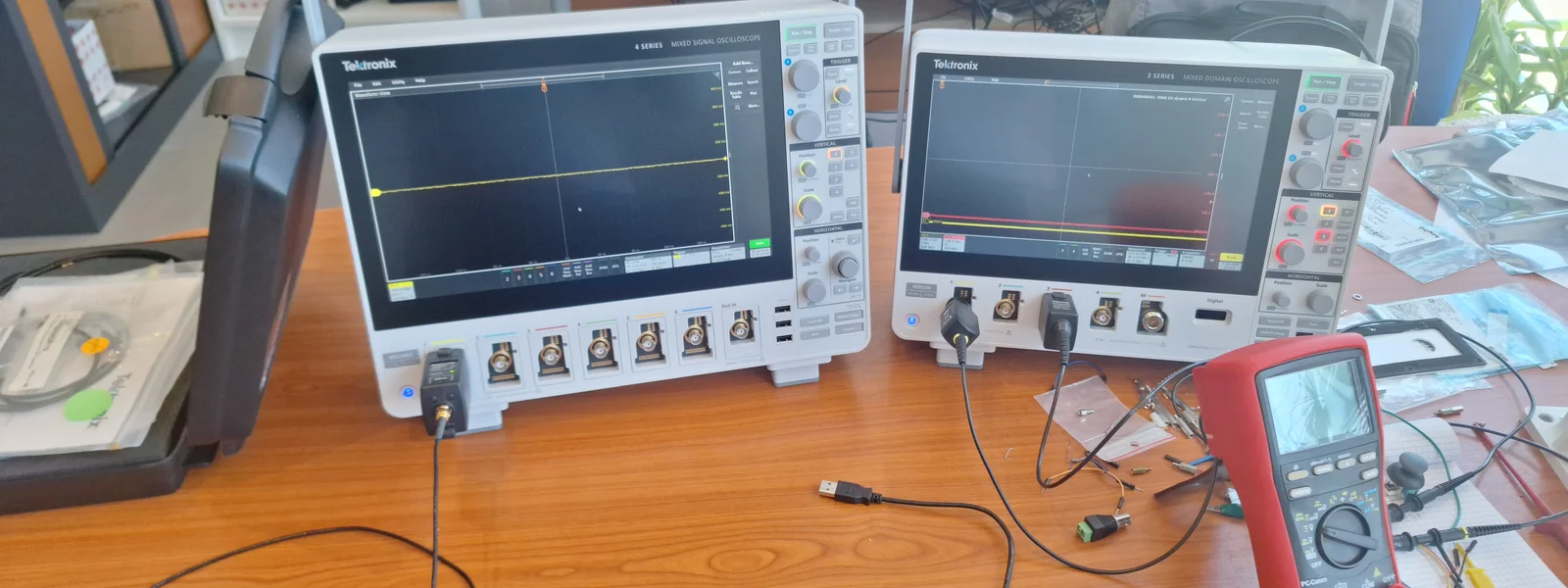
After fabrication, measurement confirms: we have a Tektronix oscilloscope equipped with the TekExpress suite, capable of running PCI Express, SATA, MIPI, USB 2/3, DDR2-4, HDMI, Ethernet and LVDS compliance tests, and helping tune equalizers to pass certification. Keysight VNA for RF, -40/+85 °C climatic chamber for temperature validation. This simulation + measurement chain explains our 100% CE/FCC certification success rate. See our articles: High-speed design, Electromagnetic compatibility.
RF up to 10 GHz, smart meter, industrial IoT, radio
RF design requires skills distinct from digital: impedance matching, microstrip / stripline lines, stage isolation, substrate choice (FR4 up to 2 GHz, Rogers beyond), PA thermal management. We routinely design sub-GHz radio modules (LoRaWAN, Sigfox, NB-IoT) up to 2.4 and 5 GHz bands (Bluetooth 5.4, Wi-Fi 6E).
We have led several RF projects up to 10 GHz. We regularly work on LIDAR, radar and SDR (Software-Defined Radio) projects. For associated certifications (ETSI EN 300 328, FCC Part 15, ARIB STD-T108), we deliver technical file elements in parallel with development. See our articles: RF design and antennas, Bluetooth, LoRaWAN, NB-IoT, Sigfox.
EMC pre-compliance from schematic
EMC doesn't get fixed late in the project. It's designed in. Our schematics integrate from the start correctly sized power filters, mastered ground returns, shielding at critical interfaces, and ESD/overvoltage protection at exposed inputs.
Measurable result: across dozens of campaigns run over more than 10 years of practice, anechoic chamber pass happens without rework. If a template overshoot appears, it's at -3 dB, fixable with an added SMD capacitor, not at -15 dB which would require a PCB re-spin. Our portfolio covers HDI technologies (laser µVias, buried vias), flex and rigid-flex formats, and printed antennas for RF applications.
High voltage and power: 10 kV, high-power supplies, motor control
Power electronics hardware design brings failure modes the digital side never sees: switching noise that lands straight in the EMC result, thermal derating that drives component choice, and isolation distances that fix the board outline before the schematic is closed.
We have developed a 10 kV high-voltage supply and worked on several high-power supplies. We also designed a multi-axis stepper motor controller with jerk-limited motion profiles, for applications where residual vibration has to stay very low. Power stages get the same treatment as the rest of the board: return paths and switching loops drawn on the schematic, derating checked against the manufacturer curves rather than the headline rating, and thermal behaviour validated in our climatic chamber.
FAQ
- Do you work with Chinese or European manufacturers?
Both. We adapt the manufacturer choice to target volume (low-volume Europe, mid-volume mix, high-volume Asia), IP constraints and industrial requirements. For medical and defense projects, we favor European manufacturers certified ISO 9001 / IATF 16949. For high-volume consumer products, Asia (China, Vietnam) remains competitive with an audited manufacturer. See our article: Outsourcing in China vs Europe.
- Can you take over an existing design to get it through certification?
Yes, it's even one of our typical electronics design consulting engagements. We first conduct a technical review (schematic, routing and component choice analysis), identify EMC/RF weaknesses, and propose either targeted fixes (partial re-spin) or a complete redesign depending on cost/benefit. The initial diagnostic takes 3 to 5 days. See: Taking over a failing electronics project.
- What's your frequency limit?
Mastered RF design up to 10 GHz. Beyond (mmWave 24-77 GHz, radar / 5G applications), we work in extended team with a specialized partner. The PCB manufacturing chain changes radically there (substrates, tolerances), even though our ANSYS HFSS simulation tools remain the same.
Hugues' understanding of the electronic behaviors at the device level is just impressive. He's one of the few hardware engineers who understand digital communications from an analog standpoint. I'd recommend him blindfolded to any prospective employer or business partner looking after quality hardware engineering.
Firmware
Industrial firmware isn't a script that works on delivery day. It's a system that has to keep running after ten years of series production, support secure OTA updates, and withstand a regulatory environment that keeps moving (CRA, IEC 62443).
Industrialization
The classic trap: a working prototype that needs six months and a re-spin to hold up in series production. At AESTECHNO, our technical signature is the opposite. DFM, IPC standards and testability are integrated into the initial schematic. The prototype is already a manufacturable board. Our designs reach series production with no industrialization rework phase: 100% success rate on CE/FCC certifications at first pass, across dozens of campaigns run over more than 10 years of practice.
Medical
Designing a medical device isn't about retrofitting an industrial board. It's about embedding patient safety, software traceability and risk management into every architectural decision, from specification to MDR technical file. At AESTECHNO, with 10+ years of experience and 65 projects since 2022, we've developed medical-class specialized lighting and designed numerous products compliant with CE and international standards.