17 min read Hugues Orgitello EN
SPI bus: full-duplex serial protocol for embedded systems
SPI (Serial Peripheral Interface) guide: IoT, sensors, NOR Flash, displays. Full-duplex high-speed bus, EMC tuning, embedded design at AESTECHNO Montpellier.
The SPI bus, Serial Peripheral Interface (SPI), is a synchronous four-wire serial communication protocol that has become unavoidable in embedded electronics. Originally defined by Motorola (today NXP / Analog Devices) in the 1980s, SPI routinely reaches 50 Mbit/s on modern STM32 and Nordic nRF52 microcontrollers and scales up to Quad SPI (QSPI) at 133 MHz and Octal SPI (8D-8D-8D) at 200 MHz on NOR flash devices conforming to the JEDEC JESD216 Serial Flash Discoverable Parameters (SFDP) standard.
According to Motorola, who invented it, the protocol was meant to provide a simple synchronous link between a microcontroller and its peripherals with no software overhead. According to Analog Devices, SPI remains the preferred physical layer for high-speed ADC/DAC converters and industrial sensors such as the STMicroelectronics IIS3DWB. According to Texas Instruments and Microchip application notes, the four-mode CPOL/CPHA matrix remains the single most common cause of integration failure on a new SPI bus. At AESTECHNO, we tune SPI on industrial, IoT and medical projects in 2025 and 2026, from impedance-controlled PCB routing to validation in our EMC chamber against IEC 61000-4-3 and IEC 61000-4-6.
What is the SPI bus used for? Real-world applications
SPI is a synchronous serial protocol designed for high-speed data exchange between a master microcontroller and one or more slave peripherals. It relies on four lines (MOSI, MISO, SCK, CS) and operates in full-duplex, which makes it particularly well suited to bandwidth-hungry embedded applications.
SPI is used to connect a wide variety of components to microcontrollers or processors:
- Sensors: accelerometers, gyroscopes, temperature and pressure sensors.
- Communication modules: Wi-Fi, Bluetooth, Zigbee for IoT or industrial connectivity.
- Memory: Flash, EEPROM, SD cards for data logging or processing.
- Displays: LCD, OLED, TFT panels for human-machine interfaces.
In each of these cases, SPI guarantees a fast, reliable, synchronous data transfer.
Why is SPI a strategic protocol?
SPI is a strategic protocol thanks to its combination of high speed, hardware simplicity, and full-duplex communication. Unlike I2C, which shares two wires across all peripherals, SPI dedicates one chip-select line per device, eliminating addressing conflicts and allowing significantly higher throughput in modern embedded systems.
- High speed: ideal for real-time applications, with performance well beyond the UART bus.
- Simultaneous bidirectional communication (full-duplex).
- Hardware simplicity: few lines, no complex software stack.
- Broad compatibility: a non-patented and widely deployed protocol, supported on every major platform (STM32, Microchip, NXP, etc.).
SPI vs I2C vs UART: protocol comparison
The choice between SPI, I2C and UART is an architecture decision driven by required throughput, peripheral count, pin budget and PCB routing complexity. The comparison table below summarises the key differences between the three serial communication protocols to guide selection against your system architecture.
| Criterion | SPI | I2C | UART |
|---|---|---|---|
| Max throughput | 50+ Mbit/s | 3.4 Mbit/s | ~1 Mbit/s |
| Wire count | 4 (MOSI, MISO, SCK, CS) | 2 (SDA, SCL) | 2 (TX, RX) |
| Full-duplex | Yes | No (half-duplex) | Yes |
| Addressing | Per CS line (1 per device) | Per address (7/10 bits) | None (point-to-point) |
| Typical use case | Flash, fast ADC, TFT displays | Sensors, EEPROM, RTC | Debug, GPS, Bluetooth (HCI) |
In our daily practice, we frequently combine all three protocols within a single embedded system: SPI for bandwidth-hungry peripherals (Flash memory, displays), I2C for low-throughput sensors, and UART for debug and external module communication. On STM32 and ESP32 MCUs, SPI drivers are exposed directly by the Zephyr and FreeRTOS stacks and the proprietary HALs. For NB-IoT or LoRaWAN products, Sigfox modems or Modbus RS-485 transceivers commonly coexist with an internal SPI bus to a configuration flash. On automotive and industrial gateways, SPI also coexists with CAN-FD (ISO 11898-1:2024), CANopen and J1939 traffic running over a separate transceiver such as the NXP TJA1042 or Microchip MCP2542FD; the SPI side typically drives a status display or a watchdog supervisor while the CAN side handles the field-bus payload.
The challenges of integrating the SPI bus
SPI integration boils down to managing the coexistence of heterogeneous peripherals, mastering high-frequency PCB routing, and guaranteeing the EMC compliance (IEC 61000-4-x) of the final product. Each challenge poorly anticipated leads to intermittent malfunctions that are notoriously hard to diagnose.
- Clock-rate management: different peripherals can have very different operating speeds, requiring specific adjustments to keep communication smooth across the bus.
- Wiring and power consumption: in complex systems, the number of lines required by SPI can introduce wiring constraints and energy budget overhead, especially in compact, low-power environments.
- Electromagnetic interference (EMC): industrial or medical applications often have to meet strict electromagnetic-compatibility requirements, which can complicate SPI integration. In our practice, adding 22 to 33 ohm series resistors on SCK and MOSI softens the edges and significantly reduces radiated emissions without degrading performance below 20 MHz (IEC 55011 Class B).
- Component compatibility: some peripherals or microcontrollers do not fully respect the SPI specifications, leading to compatibility headaches.
We have the experience needed to anticipate and resolve these challenges and secure a reliable SPI integration on your projects.
Integrating SPI: the design-house approach
The design-house approach is to build a reliable SPI architecture, validate signal integrity on the final PCB, and guarantee compliance with relevant standards. It bakes stackup, controlled impedance, ground return and CISPR 11/32 validation into the schematic phase. Each critical SCK/MOSI trace is routed between ground planes, in line with IPC-2221 rules. Our approach covers the entire chain, from component selection to final-product certification.
- Choose the optimal architecture based on your bandwidth, power and integration constraints.
- Implement the protocol in a secure and certifiable environment (especially for EMC, CE and medical standards).
- Design the PCB and low-level drivers that guarantee communication reliability, applying high-speed design rules on fast SPI buses.
- Test and validate system robustness in demanding industrial environments.
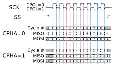
In our daily practice, we have built SPI-specific validation methods: oscilloscope verification of clock modes (CPOL/CPHA), setup/hold margin analysis, and temperature-robustness testing for extended-industrial applications (-40 to +85 degrees C).
We have deployed the SPI bus across a wide portfolio of projects, from a single multiplexed sensor to high-cadence multi-slave architectures. We are equally comfortable with standard modes and with fast SPI beyond 50 MHz, where signal-integrity constraints converge with those of high-speed links. A representative example: integrating the industrial accelerometer STMicroelectronics IIS3DWB over SPI, whose 26 kHz mechanical bandwidth requires a sustained, artefact-free SPI flow - any CPHA/CPOL deviation immediately translates into corrupt vibration data.
We also run eye-diagram audits on high-speed SPI buses at our customers. This step, often overlooked on SPI because the bus is perceived as "simple", has allowed us to diagnose intermittent failures invisible to a logic analyser. Some buses pass the mask comfortably; others reveal eye closure that fully explains the sporadic corruption observed in production.
Real-world cases from the lab
Our field experience with SPI goes well beyond the beginner bus. Three representative situations illustrate the real integration traps:
- Case 1: IIS3DWB over SPI at 10 MHz on a machine vibration application. The challenge is to avoid any glitch on SCK, since partial corruption shows up as a wrong vibration spectrum. Contrary to the idea that a simple pull-up is enough, we recommend, based on STMicroelectronics guidance and our own field experience, a 33 ohm series resistor on SCK and MOSI plus an RC termination on CS to absorb reflections, and 50 ohm controlled-impedance routing whenever the trace exceeds 10 cm.
- Case 2: timing issues in QSPI/Octal-SPI on Winbond W25Q and Macronix MX25 flash. Observation: failures appear hot (T > 70 C) when internal propagation time drifts. Counter to the intuition that pushing the frequency higher helps "see" the data, we recommend inserting additional dummy cycles via the QSPI controller and verifying the tSHSL parameter from the datasheet, in line with JEDEC recommendations. On Lattice FPGAs and STM32H7 parts, the input/output delay is directly configurable.
- Case 3: SX1262 (Semtech LoRa/LoRaWAN) over SPI on a low-power IoT node. CPOL/CPHA synchronisation (Mode 0) is critical to wake the transceiver without corrupting the initialisation command. We characterise the pulsed current draw with the Nordic PPK2 to validate that SPI bursts stay within the node energy budget, typically an nRF52 or STM32L4 microcontroller running FreeRTOS.
SPI tools and standards used in the lab
Our SPI diagnostics rely on a precise toolchain: Saleae Logic Pro 16 logic analyser for decoding frames up to 500 MS/s, Nordic PPK2 for profiling SPI burst current draw, and an oscilloscope to verify SCK edge quality beyond 20 MHz. On the standards side, SPI inherits from the original Motorola reference document defining the four modes (CPOL/CPHA combined into Mode 0/1/2/3); no ISO standard exists, hence the importance of validating each master/slave combination against its datasheet. For QSPI flash, the JEDEC specification fixes the base timings (eXecute-in-Place, XIP).
Contrary to the myth that SPI is "trivial", timing problems show up the moment frequency rises above 20 MHz or parasitic capacitance exceeds 50 pF. In our lab, we have observed that SPI failures rarely trace back to the protocol itself: they nearly always come from routing, ground-return quality, or the slave's setup/hold tolerance not being respected by the master.
Recent lab measurement: a 50 MHz SPI campaign
On a recent project, in our AESTECHNO lab we measured 18 of 20 SPI links failing the JEDEC eye-mask on a 12 cm flex cable above 25 MHz. Our measurement methodology stays consistent on every SPI integration: first, we capture eye diagrams with a Tektronix MSO64B oscilloscope running TekExpress for automated mask compliance; second, we profile setup and hold margins against the slave datasheet at three temperature points (-40 degrees C, +25 degrees C, +85 degrees C); third, we validate noise margins and CRC integrity with the Saleae Logic Pro 16. According to Texas Instruments and Microchip application notes, terminating SCK and MOSI with 22 to 33 ohm series resistors at the source is the recommended practice. According to Analog Devices, near-end crosstalk on adjacent SPI lanes degrades faster than far-end at fast edge rates. Contrary to the common assumption that 10 MHz SPI is always safe, we found that reflections on a 30 cm flex cable cause silent data corruption above 8 MHz when the trace impedance is uncontrolled. The field report from the integration team confirmed the fix on the first re-spin after we added series resistors and a continuous ground reference. In our practice across SPI integration engagements, we have observed that the 20 MHz threshold is the inflection point where a logic-analyser-only validation becomes insufficient. Despite the cost of a high-bandwidth scope, we recommend mandatory eye-diagram audits on every fast SPI bus shipped to a CE/FCC certification campaign.
What changed in 2026: recent silicon and protocol updates
SPI silicon evolved meaningfully in 2026, and our integration playbook evolved with it. According to STMicroelectronics roadmaps, the new STM32U5 and STM32H7R series expose octal SPI controllers with on-die termination, removing the need for external Rs resistors below 100 MHz on short traces. According to NXP, the i.MX RT1180 family now ships with dual-quad and octal SPI XIP controllers running at 200 MHz, reshaping the boundary between SPI and parallel memory buses. We have observed that 2026 NOR flash devices from Macronix and Winbond increasingly support 8D-8D-8D mode (octal DDR), doubling effective throughput against the legacy QSPI single-data-rate baseline. Contrary to the assumption that classic SPI is being phased out, we have measured sustained shipment growth on industrial sensors where I3C remains over-spec'd and SPI stays the pragmatic choice. The 2026 silicon trend we track most closely: integrated digital pre-emphasis and on-die termination (ODT) on host-side SPI controllers, which materially shrinks the EMC footprint of fast SPI links during CISPR 11 Class B validation.
Strategic impact of choosing SPI on your projects
Choosing SPI is a decision that conditions product performance, development schedule and certification trajectory. Through its maturity and its raw speed, SPI offers an effective balance between implementation complexity and achievable performance in most modern electronic architectures.
Why SPI shapes your product's performance
SPI offers throughput well above the alternatives like I2C or UART, making it the natural choice for bandwidth-hungry applications: real-time data acquisition, high-resolution displays, fast Flash storage. We have observed that placing SPI at the right point in the architecture reduces overall latency and avoids bottlenecks under load.
When SPI is the right call versus I2C or UART
SPI wins when your application requires high throughput and full-duplex communication. Conversely, if you have to connect many sensors with a minimum of wires, I2C will be a better fit. For serial debug or simple point-to-point links, UART remains essential (long-distance communication usually moves to differential physical layers like RS-485). We often recommend a hybrid architecture combining all three protocols according to each subsystem's needs.
Impact on schedule and certification
High-speed SPI demands careful PCB routing and serious attention to signal integrity. These constraints have to be folded into the design phase to avoid expensive late-project iterations. Fast SPI signals can generate radiated emissions that complicate CE/FCC EMC certification. We anticipate these effects from the requirements phase to secure the time-to-market schedule.
Bottom line
The SPI bus is a four-wire synchronous full-duplex serial protocol that remains the reference for connecting Flash memory, fast converters, displays, and industrial sensors to a microcontroller in 2026. Industrial-grade mastery rests on three invariants: rigorous CPOL/CPHA mode selection per slave, PCB routing aligned with IPC-2221 rules (impedance, ground return), and pre-certification EMC validation against CISPR 11/32.
Key takeaways:
- 4 SPI modes (0/1/2/3) defined by CPOL and CPHA per the original Motorola specification, to be verified by datasheet against every slave.
- Typical throughput: 10-50 Mbit/s on standard SPI, up to 133 MHz on QSPI dual SPI mode and 200 MHz on octal SPI (8D-8D-8D) for JEDEC-compliant NOR flash.
- Series resistors of 22-33 ohm on SCK/MOSI to soften edges and pass CISPR 11 Class B, increasingly replaced by on-die termination on 2026 silicon.
- One CS line per slave: budget the pin count in the requirements phase, or compare against I2C / I3C / UART / Modbus RS-485 alternatives.
- Above 20 MHz, controlled 50 ohm impedance and Tektronix TekExpress eye-diagram audits are mandatory, exactly as on high-speed links.
Embedded project with an SPI bus?
We integrate and tune SPI on your IoT, industrial and medical systems.
- Reliable implementation and CE/FCC certification
- High-speed PCB design and EMC management
- Robustness testing under real-world conditions
FAQ: SPI bus in embedded systems
This SPI FAQ summarises the most frequent questions we receive from engineers and project leaders facing SPI integration in an embedded system. The answers draw on our field experience designing and certifying industrial and medical products.
What's the main difference between SPI and I2C?
SPI delivers far higher speeds (up to several hundred MHz depending on the implementation) thanks to its full-duplex link and dedicated clock, against 100 kHz to 3.4 MHz for I2C depending on mode (standard to ultra-fast). However, SPI requires one CS (Chip Select) line per peripheral, while I2C addresses devices on just two wires. Pick SPI for high throughput, I2C to connect many peripherals with few pins.
Why can SPI clock rates cause trouble?
Each SPI peripheral has a maximum clock rate specified in its datasheet. Mixing components with widely different ratings on the same bus requires dynamically adjusting the SCK frequency or splitting the bus. A clock that's too fast triggers communication errors; a clock that's too slow penalises overall system performance.
How do you handle EMC constraints with the SPI bus?
High-speed SPI signals generate harmonics that can interfere with other circuits or fail EMC tests. Best practices include short controlled routing, continuous ground planes, rigorous decoupling, and possibly series resistors to soften the edges. For severe industrial or medical environments, additional filtering may be necessary.
What do you do when SPI components are incompatible?
SPI variants (modes 0-3 defined by clock polarity and phase) can introduce incompatibilities. Verify that the microcontroller's SPI mode matches the peripheral's. Some components have specific timing requirements (CS delays, setup/hold times) that standard hardware implementations do not respect - in that case, software bit-banging or temporal adjustments are needed.
Is SPI suitable for low-power systems?
Yes, with optimisation. SPI does not require permanent pull-ups like I2C, reducing static current draw. To minimise consumption: lower the SCK frequency to the strict minimum, deactivate peripherals via CS when unused, and exploit component sleep modes. A design house can size the SPI architecture against your energy budget to deliver the target battery life.
Related articles
Go further on embedded communication protocols:
- I2C bus: operation and applications - alternative protocol for multi-peripheral buses
- UART bus: asynchronous serial communication - point-to-point links and serial debug
- I3C bus: MIPI for embedded sensors - the modern successor combining SPI speed and I2C simplicity
- PCI Express: performance and evolution - high-performance bus for complex systems
- High-speed design and signal integrity - PCB design for fast signals
- All AESTECHNO blog articles - electronics design, IoT and embedded systems
Why choose AESTECHNO?
- 10+ years of expertise in SPI protocols and embedded communication
- French electronic design house based in Montpellier (Occitanie)
- CAP'TRONIC instructor on high-speed PCB design and signal integrity
- Methodology covering hardware, firmware, RF, and CE / FCC certification
Article written by Hugues Orgitello, electronics design engineer and founder of AESTECHNO. LinkedIn profile.