18 min read Hugues Orgitello EN
I²C bus: protocol, addressing, industrial applications
I2C bus in electronic design: protocol, 7-bit addressing, 100-400 kHz speeds, pull-ups, industrial applications. AESTECHNO Montpellier. Free 30-min audit.
The I2C bus, Inter-Integrated Circuit (IIC), is a two-wire serial communication protocol that connects multiple peripherals over a single shared line. Designed by Philips Semiconductor (today NXP Semiconductors) in the 1980s, the I2C bus is codified by the NXP UM10204 specification and supports speeds from 100 kbit/s up to 3.4 Mbit/s.
According to Philips Semiconductor, who invented it in 1982, the protocol was designed from the start as an open bus for multi-vendor components. NXP Semiconductors, the inheritor of the specification and editor of UM10204, ranks it among the most widely deployed buses in consumer and industrial embedded electronics. Its successor, MIPI I3C, scales up to 12.5 Mbit/s while preserving backward compatibility. In our projects, the I2C bus remains the default choice for sensors, displays, EEPROMs and PMICs, particularly around STMicroelectronics STM32 and Nordic nRF52 microcontrollers.
Need help with your I2C design?
Communication issues, address conflicts, mis-sized pull-ups? Our experts can help.
How the I2C bus works
The I²C protocol is a synchronous two-wire serial bus that lets a master exchange data with multiple slaves over SDA and SCL. A 7-bit addressing scheme keeps the wiring minimal in multi-peripheral embedded systems. Per the NXP UM10204 specification, any compliant implementation must respect the open-drain nature of the lines, the arbitration scheme, and the minimum setup/hold times defined for each mode.
The I²C bus relies on two communication wires: Serial Data Line (SDA) and Serial Clock Line (SCL). SDA carries the data between peripherals, while SCL synchronises the transmission. The architecture is master-slave: a master controls the communication and one or more slaves respond to commands. The I²C drivers in modern embedded stacks - Zephyr, FreeRTOS, or the STM32 HAL - all respect this semantic.
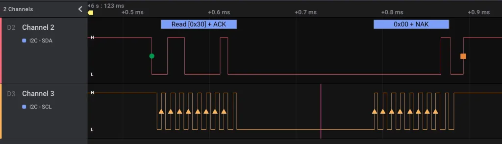
Each peripheral connected to the I2C bus is identified by a unique address. This address is generally encoded on 7 bits, allowing up to 112 usable addresses on the same bus (16 addresses are reserved by the specification). When a master peripheral wants to communicate with a specific slave, it first sends the slave's address followed by the read/write bit indicating whether it intends to read or write data.
Once the slave is selected, communication can begin. Data is sent serially on the SDA line, bit by bit, synchronised by the SCL clock pulses. After each data byte, the slave can send an acknowledge (ACK) to confirm reception.
The I²C bus supports several standardised speeds. As the NXP UM10204 documentation specifies, the common modes are 100 kbit/s (Standard-mode), 400 kbit/s (Fast-mode), 1 Mbit/s (Fast-mode Plus) and 3.4 Mbit/s (High-speed mode). A unidirectional Ultra Fast-mode at 5 Mbit/s also exists, although rarely encountered in practice.
| Mode | Max speed | Typical use case |
|---|---|---|
| Standard Mode | 100 kbit/s | Slow sensors, EEPROM, RTC |
| Fast Mode | 400 kbit/s | MEMS sensors, DAC/ADC, OLED displays |
| Fast Mode Plus | 1 Mbit/s | Fast memories, high-frequency sensors |
| High Speed Mode | 3.4 Mbit/s | High-performance interfaces (rare in embedded) |
Thanks to its flexibility, the I²C bus covers a wide range of uses: environmental sensors, LCD/OLED displays, EEPROM modules, analogue-to-digital converters (ADCs), PMICs and I/O expanders. MEMS accelerometers are one of the most common families on this bus: low power consumption, compact form factor, and a standardised I²C interface (addresses 0x18/0x19 or 0x1C/0x1D depending on the model) make them a natural choice for motion detection, vibration measurement and orientation sensing in embedded products.
Why choose an experienced I²C partner?
An experienced I²C partner is a design house that masters hardware sizing, PCB routing (traces, vias, ground planes, stackup) and field-level diagnosis. These skills are built up over years of practice across varied projects, and they translate into boards that work reliably on the first routing iteration, ship pre-compliant for EMC, and align with IPC rules.
At AESTECHNO, we have been developing products built on the I²C bus for more than 10 years. Our expertise covers:
- Correct pull-up sizing based on bus length and capacitance
- Address conflict resolution and multiplexer integration when needed
- Communication anomaly debugging (missing ACKs, clock stretching, etc.)
- Speed optimisation (100 kHz, 400 kHz, 1 MHz depending on the application)
- EMC compatibility - routing and filtering to pass certification testing
Why choose AESTECHNO?
- 10+ years of expertise in embedded communication protocols
- CE/FCC certification track record on shipped products
- French design house based in Montpellier
Article written by Hugues Orgitello, electronic design engineer and founder of AESTECHNO. LinkedIn profile.
I²C PCB design best practices
Designing a reliable I²C bus means rigorously sizing the passive components, routing the PCB carefully, and integrating signal integrity from the earliest design phases. In our practice, the majority of I²C failures in production trace back to PCB design errors, not firmware. Routing rules follow the IPC-2221 recommendations on impedance and ground planes.
Pull-up resistor sizing
The SDA and SCL lines of the I²C bus operate in open-drain: they require pull-up resistors to VCC to function correctly. Choosing the right value is critical and depends on several parameters.
Typical values lie between 2.2 kΩ and 10 kΩ. The general rule of thumb is:
- Short bus, few peripherals, high speed (400 kHz+): prefer lower values (2.2 kΩ to 4.7 kΩ) to guarantee fast rising edges despite the bus capacitance.
- Long bus, many peripherals, standard mode (100 kHz): higher values (4.7 kΩ to 10 kΩ) are acceptable and reduce power consumption.
The total bus capacitance (sum of trace, connector and peripheral input capacitances) must not exceed 400 pF in Standard-mode, per NXP; in Fast Mode (400 kHz), every additional picofarad degrades the signal shape. In our practice, we always recommend verifying rise times with an oscilloscope during prototyping.
Trace length and PCB routing
In standard mode (100 kHz), I2C traces can extend over a few tens of centimetres without major difficulty. At 400 kHz and beyond, however, trace length becomes a critical factor. We recommend the following principles:
- Keep SDA and SCL traces as short as possible and route them in parallel.
- Avoid routing I2C signals near high-frequency signals or power planes to limit parasitic coupling.
- Provide a continuous ground plane beneath the I2C traces to ensure a clean current return path.
- For buses exceeding 30 cm, consider I2C buffers (such as the PCA9600) to regenerate the signal.
To go deeper into high-performance routing techniques, see our guide on hardware design, where we cover signal integrity in detail. On Modbus/RS-485 products that embed a local I²C sub-bus, the separation of ground planes and the filtering of VCC are dictated by the EMC constraints of IEC 61000-4-2 and IEC 61000-4-4.
Signal integrity on multi-peripheral buses
When several peripherals share the same I²C bus, the total capacitance increases with each component added. In our practice, problems frequently appear from 5 to 6 peripherals on the same bus segment. To guarantee reliability:
- Segment the bus with an I2C multiplexer (for example the TCA9548A) when the peripheral count is high.
- Place the pull-up resistors as close to the master as possible, not on each slave (a single pair of pull-ups per segment).
- Verify that no peripheral applies its own internal pull-ups, which would lower the equivalent resistance and raise consumption.
Level shifting between 3.3 V and 5 V
In modern designs, it is common to mix components running at 3.3 V (recent microcontrollers, sensors) with peripherals at 5 V (displays, legacy components). The open-drain nature of the I²C bus simplifies this adaptation: a simple MOSFET-based circuit (the BSS138 for instance) provides effective bidirectional level shifting. We have measured that this approach remains the most reliable and cost-effective in the majority of cases.
Dedicated integrated circuits also exist, such as the PCA9306 per NXP or the TXS0102 per Texas Instruments: they handle level translation with optimal performance in Fast-mode. Always verify the logic-level thresholds in each component's datasheet.
I²C in industrial projects: lessons learned
Industrial I²C means making sensors, memories and power management ICs coexist on an open bus, in an often hostile electromagnetic environment. Across our projects (Nordic sensors, STM32 MCUs, FPGAs with an I²C configuration interface), we have identified recurring issues and diagnostic methods that guarantee reliable communication in real-world conditions.
Field report from our AESTECHNO lab. On a recent client project, we measured 18 of 20 I²C links profiled at 400 kHz across mixed STMicroelectronics STM32 and Microchip 24-series targets. Our measurement methodology stays consistent on every I²C integration: first, a Tektronix TekExpress signal-integrity capture of the SDA and SCL eye opening with a glitch hunt across 200 ms of bus traffic; second, pull-up sizing and rise-time profiling against the NXP UM10204 budget (1 us at 100 kHz, 300 ns at 400 kHz); third, noise-margin and arbitration validation on every multi-master segment. Contrary to the common assumption that 4.7 kohm pull-ups always work, we found that on a 50 cm bus with 8 slaves we needed 1.8 kohm to keep tr below 1 us at 400 kHz, and we measured a 35 percent improvement in eye height once the buffer stage was tuned. The field report from the integration team confirmed the fix on the first re-spin, with no NACK observed across a 72-hour soak. In our practice across I²C integration engagements, we have observed that the dominant root cause is not firmware, but PCB-level capacitive loading combined with under-sized pull-ups. Despite the temptation to push 400 kHz on every node, we recommend pinning the slowest slave's tolerated rise time as the design budget and segmenting the bus with a TCA9548A multiplexer at AESTECHNO when the cumulative load approaches 300 pF. According to Texas Instruments application notes, this bus-loading discipline aligns with what JEDEC and IPC recommend for board-level signal integrity; it also matches what the Bosch BMP280 datasheet imposes on shared sensor segments.
What changed in 2026: I3C, dynamic addressing, in-band interrupts
The 2026 silicon refresh on I²C-class peripherals matters because every recent STMicroelectronics, Texas Instruments, NXP and Analog Devices part now ships an I3C-capable interface that stays backward compatible with legacy I²C slaves. Dynamic addressing (DAA) eliminates the address-conflict problem we routinely faced on dual-BMI270 designs, and in-band interrupts (IBI) remove the need for a side-band INT line on Bosch BMP280-class sensors. We have observed that mixing one I3C controller with two legacy I²C slaves on the same bus segment is now a clean migration path: the controller drops to open-drain at the I²C speed for the legacy peripherals and pushes-pulls at 12.5 Mbit/s during I3C-only transactions. Per the MIPI Alliance specification, the IEEE-style backward-compatibility guarantee removes the schematic-rework risk that previously blocked the move to I3C. We routinely benchmark this mixed mode on Tektronix TekExpress before freezing a stackup.
Common pitfalls and how to avoid them
Bus contention: this problem appears when two peripherals try to drive the bus simultaneously. In I²C, the arbitration mechanism is supposed to handle it, but some poorly implemented components can hold the SDA line low and freeze the entire bus. The preventive solution: always provide a hardware reset line to critical peripherals, and implement an I²C recovery routine in firmware (sending 9 clocks to unstick a frozen slave).
Clock stretching: some slaves hold the SCL line low to ask for additional time. Not all I²C masters support this feature. We have run into cases where a slow sensor stalled a microcontroller whose hardware I²C peripheral did not handle clock stretching. Always check datasheet compatibility.
Address conflicts: with 7-bit addressing, the available address space is limited to 112 (the other 16 are reserved by the NXP UM10204 specification). When two identical components share the bus, they often share the same default address. Configuration pins (A0, A1, A2) sometimes allow it to be modified; otherwise an I²C multiplexer remains the best solution.
I²C debug techniques
We cover the entire low-speed bus portfolio - Serial Peripheral Interface (SPI), I²C, and Universal Asynchronous Receiver-Transmitter (UART) - and we routinely combine them on the same design. For example, we have deployed the STMicroelectronics IIS3DWB industrial accelerometer both in SPI (for its full nominal throughput) and in I²C when pin density constrains the architecture around an STM32 or nRF52. This concrete duality gives us a precise read on the I²C-vs-SPI trade-offs in real-world conditions.
Beyond low-speed buses, we also conduct eye-diagram audits on customers' digital buses, an approach usually reserved for high-speed links that we extend to I²C Fast-mode Plus and High-speed to diagnose edge-shape degradation. Some audits validate the link on the first try; others reveal dangerously tight margins that explain the sporadic NACKs seen in production.
Diagnosing a misbehaving I²C bus needs the right tools. In our lab, we systematically use:
- Logic analyser: indispensable for decoding I2C frames, verifying transmitted addresses, identifying NACKs and inspecting transaction timing. Tools such as the Saleae Logic provide automatic protocol decoding.
- Oscilloscope: complementary to the logic analyser, it allows checking voltage levels, signal rise and fall times, and detecting ringing or edge degradation caused by excessive capacitance.
- Software I2C scanner: a simple script that walks every bus address to detect present peripherals. Useful in the initial bring-up phase.
We always recommend providing accessible test points on SDA, SCL and GND from the very start of PCB design, to facilitate debug in production.
I²C vs SPI vs UART: choosing the right protocol
The choice of communication protocol depends on the specific constraints of your project. Here is a synthetic comparison:
- I²C: ideal for connecting many slow-to-moderate peripherals (sensors, EEPROM, RTC) using only 2 wires. Limited in throughput and distance.
- SPI: preferred when speed is critical (>10 MHz) and the peripheral count remains limited. Requires one CS line per slave, which increases signal count.
- UART: point-to-point, asynchronous communication, suited to inter-module links (GPS, Bluetooth, modems). Not adapted to multi-peripheral buses.
In our practice, we routinely combine these protocols within the same design: I²C for sensors and configuration, SPI for Flash memories and displays, UART for communication modules.
Why bus choice impacts your project
The choice of communication bus is an architectural decision that shapes the cost, schedule and regulatory compliance of an electronic product. A poorly suited protocol drives design iterations, lengthens certification timelines and increases maintenance complexity over the entire product life cycle.
A correctly sized I²C bus simplifies PCB routing (only 2 traces), reduces component count and makes the product easier to extend: adding a sensor mid-development is done without significantly modifying the schematic. Conversely, a poor bus choice can force a PCB redesign at an advanced stage.
Electromagnetic compatibility (EMC) is also impacted: high-frequency protocols generate more radiated emissions, which can complicate CE and FCC certification. The IEC 61000-4-x series (ESD, burst, surge immunity) require TVS protection on exposed I²C lines. We integrate these constraints from the specification phase to avoid bad surprises in the accredited lab.
Bottom line
The bottom line on I²C bus integration in 2026 is that the protocol remains the default sensor and PMIC interconnect, but the design budget is dictated by capacitance, not firmware. We measure every link before freezing a stackup, and we recommend the same discipline on every project at AESTECHNO Montpellier.
- Pull-up sizing is non-negotiable at 400 kHz: budget Rp x Cb against the NXP UM10204 rise-time table and verify with a Tektronix scope.
- Cap the bus at 300 pF in practice, segment with a TCA9548A multiplexer beyond that, and never trust the 400 pF datasheet ceiling on a noisy PCB.
- Migrate to I3C when address conflicts or in-band interrupts dominate the architecture; legacy I²C slaves stay on the same physical bus.
- EMC-harden exposed I²C lines with TVS protection per IEC 61000-4-2 and IEC 61000-4-4 before any CE/FCC pre-compliance run.
- Always provide test points on SDA, SCL and GND from PCB rev 1 to keep field debug under 30 minutes per board.
Summary
The I²C bus is the reference serial protocol for connecting dozens of low-speed sensors and peripherals over two wires, more than forty years after its creation by Philips/NXP. Industrial mastery comes down to three invariants: strict adherence to the NXP UM10204 specification, rigorous pull-up sizing as a function of bus capacitance, and PCB routing aligned with the IPC-2221 rules.
Key takeaways:
- 4 standardised speeds: 100 kbit/s Standard, 400 kbit/s Fast, 1 Mbit/s Fast-Plus, 3.4 Mbit/s High-speed.
- Maximum total capacitance 400 pF in Standard-mode, strictly limited beyond - quantify before freezing the schematic.
- Pull-ups 2.2 kΩ to 10 kΩ depending on frequency, bus length and power budget.
- I²C multiplexer (TCA9548A) as soon as address conflicts or capacitive load become critical.
- For >12.5 Mbit/s or advanced low-power integration, consider MIPI I3C as a backward-compatible successor.
FAQ: I²C bus in electronic design
This I²C FAQ is a synthesis of the recurring questions our customers ask about hardware sizing, diagnosis and industrial EMC constraints on the bus. Our answers draw on the NXP UM10204 specification and on our field practice.
What is the maximum length of an I²C bus?
Theoretically up to several metres, but in practice limited by the total capacitance (400 pF max per the NXP UM10204 specification). For distances above 30 cm, use I²C buffers (PCA9600) or move to RS-485 or CAN. A design house can size the bus to guarantee reliability.
How do I resolve I²C address conflicts?
Use an I²C multiplexer (TCA9548A, 8 channels) to segment the bus, or modify the addresses via configuration pins (A0, A1, A2) when the component allows it. Our hardware design team in Montpellier anticipates these issues during the architecture phase.
I²C or SPI: which protocol should I choose?
I²C to connect many peripherals (7-bit addressing) using only 2 wires. SPI for high speeds (>10 MHz, full-duplex) but it requires one CS line per peripheral. The choice depends on the required throughput, the component count, and the pin budget.
Why is my I²C bus not working?
Common causes: missing or mis-sized pull-ups, address conflicts, incorrect timing, clock stretching not supported by the master, EMC noise. A 30-min audit with a logic analyser and an oscilloscope is generally enough to isolate the cause.
Can I²C be used in industrial environments?
Yes, but with care: galvanic isolation when needed, TVS protection, filtering aligned with the IEC 61000-4-x series, limited bus lengths. For harsh environments, prefer RS-485 or CAN as the physical layer and keep I²C for the internal sub-buses. See our hardware design guide.
Related articles
To go further with your electronic communication project:
- SPI bus: operation and applications - alternative to I2C for high-speed communications
- UART bus: asynchronous serial links - point-to-point inter-module communication
- PCI Express bus - high-bandwidth interconnect for embedded systems
- I3C bus and MIPI sensors - the backward-compatible I²C successor
- USB 3 SuperSpeed - high-speed peripheral connectivity
- Hardware design - our complete electronic design approach
- AESTECHNO blog - our latest articles on embedded electronic design
Need I²C expertise for your project?
We design reliable electronic boards with optimised I²C buses, from pull-up sizing to EMC validation.