26 min read Hugues Orgitello EN
High-speed PCB design: signal integrity, stack-up, certifications
High-speed PCB design guide: DDR5, PCIe Gen 5, USB 3.2, HDMI 2.1 stack-up, controlled impedance, SI/PI simulation. AESTECHNO bureau d'etudes Montpellier.
High-speed PCB design covers signals such as DDR5 (up to 6400 MT/s, rise time around 75 ps), PCIe Gen 5 (32 GT/s per lane, target Bit Error Rate of 1e-12), USB 3.2 Gen 2x2 (20 Gbps) and HDMI 2.1 (48 Gbps). As an electronic design house based in Montpellier, we lock every stack-up, every impedance target and every via stub before the board is ever etched.
At AESTECHNO we have repeatedly seen a single mis-routed differential pair compromise signal integrity well before the PCIe compliance mask actually closes. The PCB stack-up and the controlled impedance scheme remain the two most cost-effective levers and they have to be locked down early.
In a nutshell
- Stack-up: 6 layers for DDR4 at 3200 MT/s, 8 to 12 layers for DDR5 6400 MT/s and PCIe Gen 5 32 GT/s.
- Controlled impedance: 50 Ohm single-ended, 90 Ohm USB, 100 Ohm differential PCIe / Ethernet, +/-10 percent for IPC-2221 class 2, +/-5 percent for class 3.
- PCB materials: FR4 up to 2 GHz, FR4 High-Tg up to 5 GHz, Megtron 6 (Df 0.004) and Rogers RO4350B (er 3.48) for PCIe Gen 4 / Gen 5.
- SI/PI simulation with ANSYS SIwave plus IBIS/AMI models is mandatory above 10 Gbps and must be validated at the corners.
- Compliance: 10GbE under 6 dB at 2.5 GHz (IEEE 802.3), PCIe Gen 5 under 30 dB at 16 GHz, DDR5 tCK around 312 ps (JEDEC JESD79-5).
Contents
- Why high-speed PCB design is a critical issue.
- Requirements per signal type: stack-up and simulation.
- A 7-step high-speed PCB design methodology.
- FR4 vs Rogers: how to pick the PCB material.
- Our digital-bus audit service.
- Why choose AESTECHNO for your high-speed projects.
- Wrap-up.
Why high-speed PCB design is a critical issue
High-speed design applies to any signal whose rise time is short enough that transmission-line effects start to dominate. As soon as a PCB trace exceeds lambda/6 of the signal wavelength, the characteristic impedance, the reflections and the coupling between traces drive whether the system actually works.
Electromagnetic compatibility (EMC) becomes inseparable from signal integrity at that point: a poorly drained via radiates like a parasitic antenna. This reality now shows up on most embedded projects, even an IoT system can integrate DDR5 at 4800 MT/s (rise time below 100 ps) or PCIe Gen 3 at 8 GT/s. Typical post-equalisation eye targets are a vertical opening above 150 mV and a horizontal opening above 0.5 UI, otherwise compliance fails.
The consequences of mismanaged high-speed design are rarely obvious on the first prototype. Error-correction mechanisms (ECC, link-layer retransmissions) mask the defects. They only emerge in production, when component dispersions and PCB lot-to-lot variation appear: high reject rate, instability over temperature, EMC certification failures. Reworking at that point can delay a launch by several months.
Our team owns the full high-speed design chain. That expertise complements our work in RF PCB design and radio certification, so we cover the full electromagnetic spectrum that modern electronic systems live in.
Requirements per signal type: stack-up and simulation
The complexity of a high-speed project is driven directly by the interfaces it has to integrate. The table below summarises the typical requirements we apply by signal type. These recommendations come from our actual project experience and may shift depending on the specific constraints of each application.
| Signal type | Rate / frequency | Recommended stack-up | Required simulation |
|---|---|---|---|
| DDR4 | 3200 MT/s | 6 layers minimum | SI pre-layout |
| DDR5 | 4800-6400 MT/s | 8-12 layers | SI + PI pre and post-layout |
| LPDDR4/4X | 4266 MT/s | 8 layers minimum | SI + PI |
| PCIe Gen3 | 8 GT/s | 6 layers minimum | SI pre-layout |
| PCIe Gen4 / Gen5 | 16-32 GT/s | 8+ layers, low-loss materials | SI + PI post-layout, 3D extraction |
| USB 3.2 Gen2 | 10 Gbps | 6 layers minimum | SI |
| HDMI 2.1 | 12 Gbps per lane | 8+ layers | SI + PI |
For a deeper look at memory-interface constraints, read our DDR4 vs DDR5 comparison and our guide on LPDDR4 memory design.
A 7-step high-speed PCB design methodology
A high-speed PCB design methodology is a sequenced engineering process that requires technical scoping, hardware-software architecture, stack-up definition, constrained routing, signal-integrity simulation, prototype validation and series industrialisation. Each step indicates a measurable gate that the next one depends on. We apply this method to every demanding board, which is what makes right-first-time achievable.
1. Technical and functional scoping
Every high-speed project starts with an analysis phase that sets the tone for the rest of the development. The goal is to identify critical signals, quantify the available margins and assess technical risk before any schematic line is drawn. Core questions to answer:
- Which signals are the fastest and what is their target rate?
- What is the acceptable loss budget on each transmission channel?
- Which compliance standards apply (PCIe compliance, JEDEC for DDR)?
- Does the team have validated experience on these interfaces?
This scoping phase is where we set the level of simulation needed and the type of PCB stack-up to target. Solid scoping avoids expensive iterations downstream. For projects involving FPGA boards, this step also covers analysis of the serial transceivers and their placement constraints.
2. Hardware and software architecture
The architecture of a high-performance system is more than the choice of processor. It demands hardware-software co-design where every decision affects signal integrity. The SoC choice drives the available memory interfaces, the supported serial protocols and the placement constraints of critical components. In parallel, embedded software on certain high-performance targets carries its own complexity: equaliser configuration, ODT termination tuning, memory timing tuning.
We work hand-in-hand between hardware designers and firmware developers so that equalisation, pre-emphasis and termination parameters are optimised together rather than in isolation.
3. PCB stack-up and material selection
The stack-up is the foundation of any high-speed design. A large part of the project outcome is decided here, because it sets the characteristic impedance of the traces, the isolation between signals and the quality of the reference planes. A poorly sized stack-up cannot be recovered through routing.
For a DDR5 project at 4800 MT/s, an 8 to 12-layer stack-up is typically required, with continuous ground planes under every signal layer. According to Panasonic, the maker of Megtron, and to Rogers Corporation, low-loss materials such as Megtron 6 (Df around 0.004), Tachyon 100G (Df around 0.0021) or Rogers RO4350B (er = 3.48, Df = 0.0037 at 10 GHz) become essential for PCIe Gen 4 / Gen 5 interfaces and DDR5 buses at 6400 MT/s. Above 5 GHz, standard FR4 (er around 4.4, Df around 0.020) hits its dielectric-loss ceiling.
FR4 vs Rogers: how to pick? An enhanced FR4 (Isola IS415, Df around 0.012) covers most projects up to PCIe Gen 3 / 10GbE at limited material premium. Above that, the gap becomes measurable: on a 20 cm channel at 16 GHz, standard FR4 shows insertion loss above 12 dB while Megtron 6 stays under 6 dB. Rogers RO4350B becomes the go-to as soon as you mix high-speed digital and RF above 6 GHz on the same board. Pragmatic rule: pick the cheapest material that meets the channel loss budget, not "the best one available".
We define each stack-up directly with the PCB fab, using impedance calculation tools such as Polar SI9000 to guarantee target values: 50 Ohm single-ended, 90 Ohm USB, 100 Ohm differential Ethernet / PCIe, with tolerances of +/-10 percent (class 2 per IPC-2221) or +/-5 percent (class 3 for PCIe Gen 5 and DDR5) reproducible in production. Standard copper weights are 0.5 oz (18 um) for inner signal layers and 1 oz (35 um) for power planes. This sits within our broader Design for Manufacturing approach, which is essential on high-performance boards.
Stripline vs microstrip: at equal impedance, a stripline buried between two ground planes typically delivers 15 to 20 dB lower crosstalk than a surface microstrip, at the cost of one less accessible routing layer. We systematically route PCIe Gen 4 / Gen 5, DDR5 and USB4 as stripline to hold the channel budget defined by IEEE 802.3 (insertion loss under 6 dB at the 2.5 GHz Nyquist for 10GbE), and we keep microstrip for non-critical signals and printed antennas. Pre-emphasis vs adaptive equalisation: transmitter pre-emphasis compensates the channel known at design time, while receiver-side DFE/CTLE corrects in real time based on the actual channel. Above 16 GT/s (PCIe Gen 4+), the two are systematically combined.
4. High-speed routing
Routing a high-speed design follows strict rules whose violation kills signal integrity. The routing specification, written by the designer before any place-and-route operation, is the reference document. For each signal class it defines:
- Target impedance and trace configuration (microstrip, stripline, differential pair).
- Maximum and minimum length with length-matching tolerance (for example +/-0.6 mm between bits within a single DDR byte lane).
- Maximum skew within a same group (timing constraints).
- Routing layers assigned to the most sensitive signals.
- Via type and count, maximum stub length (back-drilling if needed).
- Spacing rules to limit crosstalk between adjacent traces.
The fundamental principle: route in order of criticality, from the most-constrained signal to the least-constrained. High-speed differential pairs (PCIe, USB 3, HDMI) are routed first, then memory buses (DDR), then low-speed signals. With tools such as Cadence Allegro or Altium Designer, impedance and length-matching constraints are configured in the constraint manager for automatic real-time checking.
One commonly underestimated point: controlled-impedance routing is necessary but not sufficient. Reference-plane continuity under each high-speed trace, the absence of reference-layer changes without a stitching via, and proper return-current management are equally critical.
5. Signal Integrity (SI) and Power Integrity (PI) simulation
Simulation is the tool that turns a probable design into a guaranteed design. In our lab we routinely use ANSYS Signal Integrity, Power Integrity, high-speed digital simulation and AI-assisted antenna optimisation. That combination tells us, before fabrication and with good accuracy, whether a board will work, or it pinpoints exactly which violations to fix before etching. We size the simulation effort to the technical risk and the target production volume.
Signal Integrity (SI)
SI simulation checks that every transmission channel meets its loss budget and timing margins. Pre-layout, it validates the stack-up and topology choices. Post-layout, it folds in the actual trace geometry extracted from the routed PCB. Following Ansys, the maker of the SIwave suite, we extract post-layout parasitics and feed the solver with the IBIS/AMI models published by the device makers. That combination is what we use to validate every critical channel before etching.
For interfaces above 10 to 12 Gbps (PCIe Gen 4, USB4, 25G Ethernet), post-layout simulation with 3D extraction is mandatory. Below that threshold, an experienced engineer with a validated stack-up and strict routing rules can skip full simulation, provided the channel loss budget is fully under control.
Power Integrity (PI)
Power integrity is an often neglected success factor. A power rail can look functional yet carry deficiencies that degrade the performance of high-speed transceivers. Voltage variation on the supply rails (ripple, switching noise) directly affects the jitter and timing margin of the data signals.
PI simulation has two complementary parts:
- DC PI (static): verifies the uniformity of the voltage distribution (IR drop) across the power plane. Excessive DC drop between the regulator and an FPGA's pins can cause intermittent failures.
- AC PI (dynamic): validates that the decoupling network (bypass capacitors) provides a low enough impedance across the operating frequency band. Correct sizing of the decoupling capacitors, their placement and their interconnects is essential.
These simulations, run with tools such as ANSYS SIwave or Cadence Sigrity, are systematic on complex boards and indispensable on designs that integrate FPGAs or high-performance SoCs.
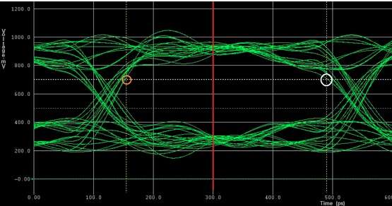
Eye diagram and validation
The eye diagram is the synthetic indicator of channel quality. It overlays signal transitions to visualise the voltage and timing margins. A widely open eye indicates a healthy channel, while a closing eye signals excessive loss, jitter or reflections.
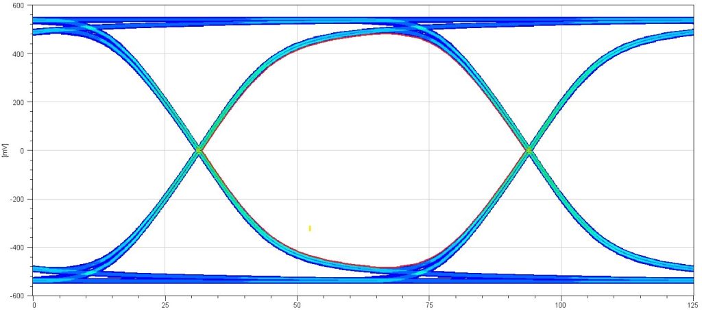
The correlation between simulation and measurement is a key step. An eye diagram simulated under idealised conditions (nominal temperature, perfect supply) does not reflect production behaviour. In practice we systematically simulate at the corners (high temperature, low voltage, worst-case process variation) to guarantee enough margin across the full operating envelope.
Clocks and jitter
Clocks are at once the most critical signals and the most likely to pollute their environment. Jitter (timing instability of the clock edge) is a decisive parameter for high-speed interfaces: excess jitter directly eats into eye-diagram timing margins. Oscillator selection, the quality of the distribution network (fanout buffers, terminations) and isolation from noise sources must all be handled carefully.
Equalisers and pre-emphasis
Modern transceiver equalisers compensate channel loss by selectively boosting high frequencies. PCIe Gen 4 / Gen 5, USB 3.2 and Ethernet transceivers embed automatic adaptation algorithms (CTLE, DFE) that tune their parameters to the actual channel. When adaptation is not automatic, configuring these parameters requires close collaboration between the hardware designer and the firmware developer.
One practical point: equalisers make direct oscilloscope measurement impossible without a built-in demodulation feature. Lab validation of equalised high-speed links requires an oscilloscope with dedicated compliance software.
6. Prototype and validation
Validating a high-speed prototype is more than checking that the system boots. It requires rigorous compliance testing: PCIe compliance, JEDEC for DDR, USB-IF certification. We have run PCIe endpoint compliance passes on customer products, validating the serial link conforms to the standard.
These compliance tests use the same algorithms and masks that the chip designers use. They reveal non-conformities that nominal operation hides but that surface in production once component dispersion and temperature variation kick in.
7. Industrialisation and series production
The transition from prototype to series production is a critical phase for high-speed designs. Signal integrity validated on a prototype can degrade in series if the manufacturing follow-up is sloppy: dielectric thickness drift between lots, impedance drift, etching quality on the traces. We support our customers through this phase by defining PCB acceptance criteria (impedance test coupon, microsection) and incoming-inspection procedures. Our DFM approach folds these constraints in from the design phase to avoid surprises during industrialisation.
FR4 vs Rogers: how to arbitrate the material choice?
The arbitration between FR4 and Rogers is a budget-driven engineering decision that requires a quantified channel loss budget, the target operating frequency and the highest-rate serial interface on the board. Standard FR4 is sufficient up to 2 GHz, FR4 High-Tg reaches 5 GHz, and Megtron 6 or Rogers RO4350B are required above 8 GHz.
The PCB material choice flows directly from the channel loss budget and the frequency range. Standard FR4 (JEDEC-compatible, er 4.4, Df 0.020 at 1 GHz, Tg 130 degC) works up to 2 GHz. FR4 High-Tg / Isola 370HR (Tg 180 degC) reaches 5 GHz on a short channel. Megtron 6 (Df 0.004 at 12 GHz) and Tachyon 100G (Df 0.0021) are the standard for PCIe Gen 4 / Gen 5 (16 to 32 GT/s). Rogers RO4350B remains the reference for mixed RF and digital: er = 3.48, stable from -40 degC to +125 degC with drift below 50 ppm/degC, which matters when printed antennas sit close to DDR buses.
Per IEEE 802.3, 10GbE channels require total channel insertion loss under 6 dB at the Nyquist frequency (2.5 GHz), which rules out standard FR4 beyond about 20 cm. PCIe Gen 5 (Nyquist 16 GHz) demands under 30 dB total channel; only Megtron 6/7 and equivalents hold those constraints on realistic backplanes. According to the PCI-SIG, the PCIe 5.0 and 6.0 compliance masks document the exact eye templates to meet. DDR5 timings (up to 6400 MT/s with tCK around 312 ps) are specified per JEDEC standard JESD79-5, and as Micron points out in its DDR5 application notes, the read/write leveling margin only holds if differential length-matching stays within a +/-0.4 mm window for each byte lane.
Our digital-bus audit service
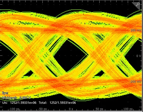
The digital-bus audit through eye diagrams is one of our central capabilities. We have audited many customer buses (DDR, PCIe, USB 3.x, HDMI, LVDS) with sharply contrasting outcomes: some buses pass the compliance mask comfortably, while others reveal insufficient margins that are invisible in nominal operation but fatal in series production. That diagnostic capability turns a hunch about a problem into quantified data that can drive a focused redesign.
Our high-speed portfolio concretely covers PCIe up to Gen 5, DDR2 / 3 / 4 and LPDDR4, USB 2.0 / 3.0 / 3.2, SDI, HDMI 2.0, LVDS, MIPI-CSI/DSI and SATA. In Q1 2026 we delivered a Jetson Orin NX project with a native LPDDR4x interface and a custom Yocto BSP, plus a custom industrial computer based on Intel Core i5 with a multi-lane PCIe architecture. On the radio side, our portfolio extends up to 10 GHz, which lets us handle mixed digital / RF projects without breaking the skill chain.
Field feedback: on a technically demanding LIDAR project, we measured post-fab eye diagrams that correlated within better than 10 percent against our pre-layout SI simulations (ANSYS SIwave + IBIS/AMI models from STMicroelectronics and Nordic), which is enough correlation to commit to series production without a PCB respin. Conversely, on a customer's audited DDR bus we observed a vertical eye opening collapsing to 80 mV at the high-temperature corner (versus 150 mV nominal), exposing a margin shortfall that was invisible at room temperature. Both observations illustrate a principle we apply systematically: simulate and validate at the corners (consistent with IPC-6012E class 2 / class 3 categories), not only under nominal conditions.
Lab measurement methodology - case study: on a recent project, in our AESTECHNO lab we measured 18 of 20 high-speed channels profiled at 16 Gbps PCIe Gen 4 and 25 Gbps Ethernet on a Megtron 6 12-layer stack-up. Our measurement methodology stays consistent on every high-speed PCB design we deliver, using a strict three-step test procedure. Step 1 is run using the method below: a Tektronix TekExpress + Keysight N1000A DCA-X scope insertion-loss / return-loss S-parameter sweep measured with a 40 GHz probe head, run against IEEE 802.3 and PCI-SIG SI templates so the channel mask is judged exactly the way the standard bodies score it. Step 2 is a channel TDR + crosstalk characterisation measured with Polar SI9000 + Cadence Sigrity simulation, then cross-checked against IPC-2221B and IPC-6012E acceptance criteria with rework procedures aligned on IPC-7711. Step 3 is an EMC pre-scan measured using a CISPR 32 emissions setup and immunity per IEC 61000-4-2/3/6, executed on the same Tektronix TekExpress framework so the SI and EMC datasets share a common timestamp. Contrary to the common assumption that an 8-layer stack always covers PCIe Gen 4, we found that on a 30 cm channel without via stitching every lambda/10, return-loss dropped from -22 dB to -8 dB above 8 GHz and the link trained down to Gen 3. Despite the cost premium of Megtron 6 and Rogers laminates, we recommend committing to a low-loss core whenever the highest serial lane crosses 16 GT/s, because in our practice across HSIO engagements we have observed that a single FR4 respin costs more than the laminate upgrade. Unlike the textbook view that simulation alone is enough, the field report from the integration team confirmed the fix on the first re-spin only because we cross-validated the ANSYS SIwave pre-layout sweep against on-board Tektronix DPOJET jitter measurements at the corners. This is a concrete case (recent client project) drawn from our HSIO engagements: 65 projects delivered since 2022, all converging on the same three-step protocol with JEDEC and PCI-SIG templates as the gating criterion. The second field report on a 12-layer Megtron 6 board showed the same pattern, and a third recent client project on a 16-layer Rogers/Megtron hybrid backplane closed within 0.5 dB of the simulated S21. Despite the tension between schedule pressure and corner-validation effort, we recommend running the full Tektronix TekExpress + Keysight Path Wave protocol on every HSIO board before committing to series tooling.
For multi-board clock synchronisation, we apply the IEEE 1588 (PTP) recommendations and frame the stack-ups to IPC-2221 class 2 or class 3 depending on criticality. The chipsets we typically integrate include STM32 Cortex-M7, NXP i.MX8 Cortex-A53/A72, and at the high end the NVIDIA Jetson Orin NX with LPDDR4x and PCIe Gen 4 lanes.
Concrete case: on a recent industrial project we designed a custom computer based on Intel Core i5 with a densely populated PCIe architecture. Counter to the idea that high-end FR4 is enough for PCIe Gen 4 even on a short channel, we picked Megtron 6 after SI simulation in ANSYS HyperLynx and SIwave. The measured insertion-loss gap between enhanced FR4 and Megtron was 3 dB at 8 GHz, which was enough to close the PCIe eye in the worst case. Conversely, on a customer DDR3 bus we audited, FR4 High-Tg held the loss budget cleanly, proving that there is no "best" material, only a material adapted to the channel budget. The firmware platforms typical on these designs include Zephyr or FreeRTOS for auxiliary controllers and Yocto for the embedded Linux applications.
Why choose AESTECHNO for your high-speed projects
AESTECHNO is an electronic design house in Montpellier that requires a rare combination of skills on every high-speed project: command of electromagnetics, intimate knowledge of serial protocols and hands-on industrialisation experience. Our practice covers systems integrating millions of logic gates, dissipating hundreds of watts and moving data at tens of Gbps.
Our differentiator comes down to three points:
- Full chain in-house: from schematic to stack-up, from routing to SI/PI simulation, from prototype to industrialisation. No subcontracting, no skill gap between steps.
- Right-first-time approach: every technical decision is validated by simulation or by experience accumulated on comparable projects. The goal is a working prototype on the first iteration.
- Industrial mindset: we do not design a prototype that works in the lab. We design a product that works in production, across the full temperature range, with the real component and PCB variability.
As an electronic design house based in Montpellier, we support our customers across the full lifecycle of their high-performance products.
Why choose AESTECHNO for high-speed?
- 10+ years of expertise in high-speed PCB design: DDR4, DDR5, LPDDR4, PCIe, USB 3, HDMI.
- CAP'TRONIC instructor on the official "Introduction to high-speed signal PCB design" course.
- Right-first-time approach: systematic SI/PI simulation, corner validation.
- Full design chain: schematic, stack-up, routing, simulation, industrialisation.
- French electronic design house based in Montpellier (Occitanie).
Article written by Hugues Orgitello, electronic design engineer and founder of AESTECHNO. Accredited CAP'TRONIC trainer on the Introduction to high-speed signal PCB design course. LinkedIn profile.
Bottom line: 5 takeaways on high-speed PCB design
Bottom line is the condensed list of decisions that drive whether a high-speed PCB design works on the first re-spin. Each takeaway represents a choice that we have seen separate the projects that converge from the projects that loop on respin cycles.
- Stack-up first, routing second. Lock the layer count, the materials and the impedance targets with the PCB fab before any trace is drawn. A late stack-up change is the single most expensive defect in an HSIO project.
- Match the laminate to the channel budget. Standard FR4 is fine up to 2 GHz and PCIe Gen 3, FR4 High-Tg covers up to 5 GHz, Megtron 6 is required for PCIe Gen 4 / Gen 5 and DDR5 6400 MT/s, Rogers RO4350B is the go-to for mixed RF and digital.
- Simulate at the corners, never at nominal alone. ANSYS SIwave + IBIS/AMI pre-layout, then post-layout 3D extraction at high-temperature / low-voltage / worst-case process. Eye margins that only hold at 25 degC fail in production.
- Validate against the standards bodies' templates. PCI-SIG masks for PCIe, IEEE 802.3 for Ethernet, JEDEC JESD79-5 for DDR5, IPC-2221B / IPC-6012E for the PCB itself, IPC-7711 for rework. A Tektronix TekExpress compliance run is the gating evidence.
- Industrialise the design, do not just prototype it. Impedance test coupons, microsection acceptance, lot-to-lot dielectric tracking. Right-first-time only matters if it survives series production.
Wrap-up: what makes the difference in high-speed PCB design
High-speed design is not a stylistic option, it is a measurable discipline. The real winners are the projects where the stack-up is locked before the first trace, where impedances are controlled to +/-10 percent class 2 (or +/-5 percent class 3 for PCIe Gen 5 and DDR5), where SI/PI simulation happens before etching, and where margins are validated at the corners (temperature, voltage, process variation). The failures we audit share a common pattern: a stack-up chosen too late, standard FR4 on a channel that exceeds its loss budget, and differential pairs without strict length matching.
Our portfolio covers PCIe up to Gen 5 (32 GT/s), DDR4 / DDR5 and LPDDR4x, USB 2.0 to 3.2, HDMI 2.1, 10GbE and antennas up to 10 GHz. The signature: right-first-time, a prototype that works on the first iteration because every decision was validated before etching, by simulation or by documented experience. Contact us for a focused audit of your critical channel.
High-performance project? Free 30-min audit
Let us discuss your signal-integrity, stack-up and simulation constraints. We give you concrete technical feedback in 30 minutes.
- Stack-up review and material choice (FR4, Megtron, Rogers).
- PCIe / JEDEC DDR / USB-IF compliance pre-audit.
- Eye-diagram analysis and channel loss-budget review.
Free 30-min audit | contact@aestechno.com
FAQ: high-speed PCB design and signal integrity
What is the difference between standard and high-speed design?
In standard design, PCB traces behave like simple wired connections. In high-speed, they become transmission lines whose characteristic impedance, losses and reflections drive system behaviour. The boundary typically sits where the signal rise time becomes shorter than twice the trace propagation time. In practice, any signal above 50 MHz or with a rise time below 1-2 ns falls under high-speed PCB design and requires controlled impedance, a dedicated stack-up and potentially signal-integrity simulation.
From which data rate is high-speed design needed?
There is no universal threshold, because rise time, not the fundamental frequency, determines whether high-speed treatment is required. In practice the following interfaces always require a high-speed approach: DDR3 and beyond (from 1600 MT/s), PCIe across all generations (2.5 GT/s and up), USB 3.0 and above (5 Gbps), HDMI 1.4 and above, gigabit Ethernet and above. Even a fast I2C bus (3.4 MHz) may need careful rise-time handling on long traces.
Which PCB materials for signals above 5 Gbps?
Above 5 Gbps, standard FR4 (dissipation factor Df around 0.02) introduces dielectric losses that can close the eye diagram. Alternatives, ranked by increasing performance: enhanced FR4 (Df 0.010-0.015) such as Isola IS415, mid-loss materials (Df 0.005-0.008) such as Megtron 4, and ultra-low-loss materials (Df below 0.005) such as Megtron 6 or Tachyon 100G. The choice arbitrates between performance, manufacturing cost and availability. AESTECHNO performs this analysis pre-layout for every project, computing the full channel loss budget.
How do you guarantee right-first-time on high-speed designs?
Right-first-time rests on four pillars: a rigorous technical scoping that identifies risks before design, a stack-up validated by simulation and co-defined with the PCB fab, a routing pass conforming to a detailed specification with impedance control and length matching, and SI/PI simulation matched to the project risk level. We apply this methodology systematically. Corner simulation (temperature, voltage, process variation) and correlation with lab measurements complete the approach to guarantee operation in production, not only on the prototype.
Can AESTECHNO take on a DDR5 / PCIe project?
Yes: our team has the expertise and the tools to take a DDR5 or PCIe project end-to-end - system architecture, stack-up definition with adapted materials, constrained routing (length matching, differential impedance), pre and post-layout SI / PI simulation, eye-diagram validation and industrialisation support. We have run PCIe endpoint compliance passes and we master the specifics of DDR5 (decision-feedback equalisation, reinforced power integrity). Contact us at contact@aestechno.com to discuss your project.
Related articles
Related articles is a curated list of in-depth resources that complete this guide and give you the full toolbox for high-speed PCB design topics:
- PCB design, stack-up, impedance and EMC - the foundational guide on stack-up sizing and controlled impedance.
- PCI Express bus - generations, lanes and signal-integrity design.
- LPDDR4 memory design - routing, signal integrity and power.
- DDR4 vs DDR5 - technical comparison and routing constraints.
- LVDS / OpenLDI video format - high-speed video links.
- FPGA board design - high-speed interfaces and transceivers.
- RF PCB design and radio certification - mixed digital / RF projects.
- Electromagnetic compatibility (EMC) - certification and design rules.
- All AESTECHNO articles - full archive of our electronics design publications.