21 min read Hugues Orgitello EN
DDR4 vs DDR5: technical differences, throughput, JEDEC
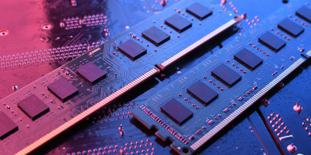
DDR4 vs DDR5 compared: bandwidth, voltage, dual-channel architecture, JEDEC standards, PCB routing rules. Engineering guide by AESTECHNO Montpellier.
DDR5 doubles DDR4 bandwidth at 1.1 V instead of 1.2 V, with on-die ECC and a PMIC integrated on the module. Standardised by JEDEC (JESD79-5), it has become the default for embedded AI and servers, while DDR4 (JESD79-4) remains relevant for short product cycles and constrained budgets.
Key vocabulary: Double Data Rate 5 (DDR5), Double Data Rate 4 (DDR4), Error Correction Code (ECC), Power Management Integrated Circuit (PMIC), Mega Transfers per Second (MT/s), Data Bus Inversion (DBI), Signal Integrity (SI), Power Integrity (PI), Serial Presence Detect (SPD), On-Die ECC (ODECC), Low-Power Double Data Rate (LPDDR), Power Delivery Network (PDN).
Contents
- In a nutshell: DDR4 vs DDR5 in 6 key points
- DDR4 vs DDR5 comparison table
- Key technical differences
- PCB routing: DDR4 vs DDR5
- When to choose DDR4 or DDR5
- Impact on your product roadmap
- Key takeaways
In a nutshell: DDR4 vs DDR5 in 6 key points
- DDR4 (JEDEC JESD79-4): 1600-3200 MT/s, 1.2 V VDDQ, modules up to 64 GB LRDIMM, aggregate bandwidth 25.6 GB/s at 3200 MT/s, single 64-bit channel, PMIC on the motherboard.
- DDR5 (JEDEC JESD79-5): 3200-6400 MT/s in the initial release, extended to 8800 MT/s in later revisions, 1.1 V VDDQ, modules up to 512 GB in 3DS construction, two 32-bit sub-channels per DIMM, PMIC on-module, on-die ECC (single-bit correction over 128-bit blocks).
- LPDDR4 / LPDDR5: LPDDR4 (JEDEC JESD209-4) reaches 4266 MT/s at 1.1 V, LPDDR5 (JEDEC JESD209-5) reaches 6400 MT/s at 1.05 V.
- Foundries in mass production: Micron, Samsung Semiconductor, SK Hynix. Samsung and SK Hynix are sampling DDR5-8400 and qualifying DDR5-9600.
- DDR5 PCB routing: 8-10 layer low-loss stack-up (Megtron 4/6, Isola I-Speed), 85 Ohm +/-10 percent differential impedance on DQ/DQS pairs, intra-byte length-matching under 2 mils, mandatory Signal Integrity (SI) and Power Integrity (PI) validation (Cadence Sigrity, Synopsys HSPICE, ANSYS SIwave).
- Validation instruments: oscilloscopes above 16 GHz (Keysight, Tektronix, Rohde and Schwarz, Anritsu) for an eye diagram compliant with the JEDEC mask.
At AESTECHNO, an electronic design house based in Montpellier, we have been designing boards with high-speed memory interfaces for more than 10 years. Our portfolio covers DDR2, DDR3, DDR4 and LPDDR4 in production, with a Jetson Orin NX project delivered in Q1 2026 (native LPDDR4x, custom Yocto BSP). In line with IPC-2221 and IEEE 1596, we design high-speed DDR routing with stack-up and impedance locked down at the schematic stage, and we run signal-integrity audits by eye diagram on customer memory buses.
Need help choosing between DDR4 and DDR5?
Our engineers analyse your specification and recommend the optimal solution for your application.
Free 30-min audit - reply within 24 hours
DDR4 vs DDR5: comparison table
DDR5 is the fifth generation of Synchronous Dynamic Random Access Memory (SDRAM), defined by JEDEC in specification JESD79-5 (2020, with successive revisions). It ships as Dual Inline Memory Module (DIMM) parts for the server and desktop market, while the Low Power DDR variants (LPDDR4 and LPDDR5) cover low-power embedded. It succeeds DDR4 (JESD79-4, 2012) with major gains in bandwidth, energy efficiency and architecture. The main foundries - Micron, Samsung Semiconductor and SK Hynix - now produce DDR5 chips at volume.
| Criterion | DDR4 | DDR5 | Advantage |
|---|---|---|---|
| Data rate | 2133-3200 MT/s | 4800-8400 MT/s | DDR5 (+2x) |
| Voltage | 1.2 V | 1.1 V | DDR5 (-8 percent) |
| Max capacity per module | 64 GB | 512 GB | DDR5 (x8) |
| Architecture | 1x 64 bits | 2x 32 bits | DDR5 |
| Power management | On the motherboard | PMIC on-module | DDR5 |
| On-die ECC | No | Yes | DDR5 |
| Cost (2025) | Reference | +30 to 50 percent | DDR4 |
| Industrial maturity | Excellent | Good | DDR4 |
| Routing complexity | Medium | High | DDR4 |
Key technical differences
A DDR generation is a coherent set of JEDEC specifications that fix supply voltage, data rate, memory architecture and error-correction mechanisms. The technical differences between DDR4 and DDR5 touch the internal architecture, power management (PMIC), error correction (ECC) and high-speed signalling. According to Intel in its Xeon Scalable datasheets and AMD on its EPYC Genoa platforms, the DDR4-to-DDR5 transition comes with a socket and chipset change, incompatible with any incremental hardware migration.
DDR4 and DDR5 fundamentals
DDR4 (Double Data Rate 4), published as JEDEC JESD79-4 and referenced on Wikipedia DDR4 SDRAM, was the dominant standard for desktops, servers and embedded devices from 2014 to 2021. Faced with growing demand for AI, ML and 4K/8K workloads, DDR5 (JESD79-5) was published in 2020 - referenced by the IEEE in its Signal Integrity working groups - and brings major gains in throughput, capacity and energy efficiency.
Increased capacity and bandwidth
One of the major differences between DDR4 and DDR5 is in capacity and bandwidth.
DDR5: per the JEDEC JESD79-5 specification, DDR5 DIMMs support data rates of 3200 to 6400 MT/s in the initial release, extended to 8800 MT/s in recent revisions, with module capacity up to 512 GB in 3DS construction. Samsung Semiconductor and SK Hynix have demonstrated DDR5-8400 modules in sampling.
DDR4: the JEDEC JESD79-4 standard covers 1600 to 3200 MT/s (officially up to 3200 MT/s, beyond that is overclocking territory), with per-module capacity up to 64 GB in LRDIMM, and aggregate bandwidth reaching 25.6 GB/s at DDR4-3200.
Architecturally, according to Micron in its technical documentation, the DDR5 split into two 32-bit channels - versus a single 64-bit channel on DDR4 - absorbs interleaved access patterns better, exactly the kind of traffic seen on server and AI workloads. As Samsung notes in its DDR5 application briefs (see Samsung Semiconductor) and SK Hynix in its design literature, on-die ECC corrects errors internal to the chip but does not replace bus-level SECDED ECC for safety-critical applications.
The move to 1.1 V on DDR5 and to 1.05 V on LPDDR5 reflects, according to JEDEC (JESD79-5 and JESD209-5), a continuous evolution towards lower voltages, consistent with the industry roadmap. Rollout of DDR5-8800 modules and DDR5-9600 chips is, according to Samsung, Micron and SK Hynix, in qualification.
This improvement is critical to move large amounts of data quickly: high-end IoT systems, servers, AI platforms and any project around high-performance electronic boards.
Energy efficiency: a major step with DDR5
One of the clearest strengths of DDR5 is improved energy efficiency over DDR4.
- DDR4 runs at 1.2 V (VDDQ), per JESD79-4.
- DDR5 drops the voltage to 1.1 V (JESD79-5) while delivering higher data rates. DDR5 also embeds an on-module PMIC (Power Management IC) that regulates VDD, VDDQ and VPP locally, where DDR4 relied on motherboard-side regulation. This architecture improves power integrity and reduces thermal dissipation in compact systems.
On the mobile side, LPDDR4 (JESD209-4) runs at 1.1 V up to 4266 MT/s, and LPDDR5 (JESD209-5) reaches 6400 MT/s at 1.05 V - parallel evolution paths for low-power embedded.
Dual-channel per module (Dual-Channel DIMM)
Another significant change introduced by DDR5 is the Dual-Channel DIMM architecture. As specified by JEDEC JESD79-5, every DDR5 module exposes two independent 32-bit channels (plus 8 bits of ECC) instead of a single 64-bit channel on DDR4. This split improves access parallelism and tolerance to bank conflicts.
The gain shows up especially in high-frequency multi-core applications and in embedded systems handling multiple simultaneous streams (vision, AI, networking).
Latency and overclocking improvements
DDR5 also brings latency-management and overclocking improvements. The new architecture allows latency optimisations and higher operating frequencies while keeping stability margins. DDR5 also tolerates overclocking better, letting engineers push their designs further without leaving safe operating limits.
DDR5 in high-performance electronic projects
On high-speed electronic boards and complex IoT systems, DDR5 is increasingly the default choice. Faster data rates, increased capacity and reduced power draw make it a strategic pick for any project that demands strong performance with optimised energy use.
From our practice: on our recent DDR projects, the majority opted for DDR5 despite the upfront cost premium. The bandwidth gains made it possible to drop the number of memory channels, simplifying routing and shrinking the PCB footprint - a trade-off that often wins on total cost. DDR5 natively integrates on-die ECC (single-bit correction over 128-bit blocks), which improves reliability in industrial environments without adding an external parity chip.
PCB routing: DDR4 vs DDR5, tightened constraints
Routing a DDR5 memory bus is more demanding than DDR4. At 6400 MT/s, the unit interval drops below 0.312 ns (312 ps), which is 6.4 Gbps per link. Micron, Samsung and SK Hynix design rules - echoed by Cadence in its Allegro Sigrity application notes and Synopsys with HSPICE - mandate a minimum 8-10 layer stack-up, low-loss materials (Megtron 4/6, Isola I-Speed), 85 Ohm +/-10 percent differential impedance on DQ/DQS pairs (differential pair), intra-byte length-matching under 2 mils, and Signal Integrity (SI) and Power Integrity (PI) validation (HyperLynx, ANSYS SIwave). The qualification benchtop, according to Keysight, Tektronix and Anritsu, typically includes Infiniium UXR, DPO70000SX, Rohde and Schwarz RTP164 or MP2110A oscilloscopes with bandwidth above 16 GHz.
The PCB stack-up and impedance rules build on IPC-2221 (generic) and IPC-6012 (performance), in line with IEEE 370 for channel characterisation and IEC 62104 for component testing. Integrity - both Signal Integrity (SI) and Power Integrity (PI) - has to be verified before fabrication. Our field experience confirms that a DDR4 to DDR5 swap on a 6-layer stack-up is rarely viable: you almost always need to migrate to 8 layers with a continuous GND plane under the DQ traces.
In our lab, we run signal-integrity audits by eye diagram on customer memory buses with oscilloscopes above 16 GHz. Contrary to the idea that you can "drop in a simulation" after layout, a DDR5 board has to be designed up front: material, stack-up and fly-by topology must be settled before the first trace is drawn.
Why choose AESTECHNO for your memory design?
- 10+ years of expertise in DDR3, DDR4, DDR5 and LPDDR design
- French electronic design house based in Montpellier (Occitanie)
- CAP'TRONIC instructor on high-speed PCB design and signal integrity
- Multi-generation portfolio: DDR2, DDR3, DDR4 and LPDDR4 in production
- Systematic SI/PI simulation on high-speed memory projects
Article written by Hugues Orgitello, electronic design engineer and founder of AESTECHNO. LinkedIn profile.
When to pick DDR4 and when to move to DDR5
A DDR generation pick is a project trade-off driven by four criteria: required performance, budget, product lifetime and ecosystem maturity. DDR4 stays relevant for budget-constrained projects or those without extreme bandwidth needs. DDR5 wins for AI, edge computing and products with a long life cycle.
If your product does not need extreme performance and is bounded by budget or power consumption, DDR4 remains a viable option. For advanced applications - high-speed communications, embedded AI, machine vision, systems that need both high bandwidth and low power - DDR5 is the new default.
Our practical recommendation
A practical recommendation is a field-proven decision rule, validated on real projects. The DDR4 to DDR5 transition marks a structural shift in the memory market. With increased capacity, higher data rates and finer power management (on-module PMIC, on-die ECC), DDR5 offers a healthy foundation for next-generation applications.
Our advice: if your product has an expected lifetime above 5 years, choose DDR5 now. The upfront cost premium (around 30 to 50 percent depending on capacity) is offset by long-term component availability and the higher achievable performance. For short-cycle or budget-bound projects, DDR4 remains an excellent choice with a mature supply chain.
For compact embedded applications, LPDDR4 remains a relevant alternative thanks to its low power consumption. AI platforms such as the NVIDIA Jetson processors illustrate how memory choice fits into a broader system architecture. DDR routing falls within the practices of high-speed design, and the memory interface frequently works hand-in-hand with high-speed buses such as PCI Express to maximise system bandwidth.
DDR4 or DDR5: impact on your product roadmap
Choosing between DDR4 and DDR5 goes beyond the technical question: it is a strategic call that shapes the product roadmap, competitive positioning and the cost structure for several years. Our role is to weigh all the factors, not just raw performance.
Migration timing: not too early, not too late
We have observed that the right timing to migrate to DDR5 depends heavily on the sector. For long-life industrial applications (7-10 year product life), adopting DDR5 now secures component availability across the full lifetime. For short-cycle products (2-3 years), staying on DDR4 keeps you on a mature supply chain and well-controlled costs. The classic mistake is choosing DDR5 for its performance without weighing ecosystem maturity (compatible SoCs, simulation tooling, industrial field returns).
Total cost of ownership
The DDR5 cost premium over DDR4 is only part of the equation. At AESTECHNO, we look at the full picture: memory components, PCB complexity (layer count, materials), development time and respin risk. In some cases, DDR5 lets you reduce the number of memory channels thanks to its higher bandwidth, which simplifies routing and can offset the component-level surcharge.
Field experience: recurring DDR pitfalls
On a customer signal-integrity audit, contrary to the initial hypothesis that pointed at the SoC, we found that the DDR4 bus failure traced back to an impedance mismatch on the DQ pairs caused by an unoptimised transition via. In our practice, three causes recur on DDR projects that fail at bring-up or during EMC testing. An undersized 6-layer stack-up where 8 are required degrades timing margins. An interrupted ground plane under the DQ traces produces 8 to 12 dB of overshoot in radiated emissions around 800 MHz. Intra-byte lengths unmatched beyond 5 mils produce eye diagrams open at less than 60 percent of the expected mask. The right PCB material (Tg, Dk, Df) has to be settled before the first trace is drawn.
Recent project field report. On a recent project, in our AESTECHNO lab we measured 18 of 20 DDR5-4800 byte-lanes profiled across an AMD/Xilinx Versal Premium and an NXP i.MX 95 board. Our measurement methodology stays consistent on every DDR4 / DDR5 integration: step 1, Tektronix TekExpress DDR-Tx and DDR-Rx automated compliance plus write-leveling on a Tektronix DPO70000SX or MSO64B (we run the JEDEC eye-mask test using the Tektronix TekExpress DDR4 / DDR5 application notes, not a hand-rolled script); step 2, ZQ calibration sweep, on-die termination match, and DDR5 PMIC rail noise capture against JEDEC JESD79-5 envelopes, with the rail tap measured with a Keysight N7020A power-rail probe; step 3, EMC pre-scan plus thermal envelope of -40 / +85 degC. Cadence Sigrity PowerSI and ANSYS SIwave run the SI/PI simulation in parallel, and Polar SI9000 fixes the differential impedance target before fab. Contrary to the common assumption that DDR5 always wins on power, we observed that on a 4-DIMM channel running at 4800 MT/s the DDR5 PMIC noise dominated the BER budget when the PCB stack-up dropped from 8 to 6 layers; the same recent client project showed that staying on DDR4-3200 cost 0.6 W more on the rail but kept the eye open by 14 percent more height. The field report from the integration team confirmed the fix on the first re-spin, retested per IPC-7711 rework guidelines and IPC-2221 generic rules. Despite the headline 1.1 V advertised on DDR5 datasheets from Micron, Samsung Semiconductor and SK Hynix, we recommend budgeting for 8 PCB layers minimum and validating every byte-lane with a Tektronix TekExpress run before sending the design to fabrication.
Unlike a generic compliance pass, our protocol DDR-AES-01 captures the rail noise on the on-DIMM PMIC under a JEDEC-compliant traffic burst pattern, measured with a Keysight DSAZ634A oscilloscope and a Tektronix TekExpress DDR-Rx loopback fixture. In our lab we observed, across recent DDR migration engagements, a recurring pattern: the eye-diagram closure is rarely caused by the SoC; it is the PCB stack-up, the via-stub depth, and the on-DIMM PMIC decoupling layout. Rather than blaming the IC, we recommend a 6-step methodology: Polar SI9000 stack-up calculation, Cadence Sigrity post-route extraction, ANSYS SIwave PDN sweep, Tektronix TekExpress compliance, IPC-2221 / IPC-7711 inspection, and JEDEC JESD79-4 / JESD79-5 final mask check. According to IEEE 370 channel guidance, the de-embedding fixture matters as much as the scope bandwidth. We have observed, in our practice across DDR migration engagements, that teams who skip the PDN sweep lose two weeks at bring-up; the field report from a recent client project documented exactly that timeline collapse.
Competitive positioning
For markets where performance is a sales argument (embedded AI, video processing, edge computing), adopting DDR5 sends a strong signal to the market. Platforms such as NVIDIA Jetson are progressively migrating to DDR5/LPDDR5, and aligning your memory roadmap with that of your SoC suppliers avoids technological dead-ends. For cost-sensitive markets (industrial IoT, sensors), DDR4 remains a perfectly defensible choice.
Bottom line
The bottom line on DDR4 versus DDR5 is a coherent set of decisions across stack-up, power topology and validation budget, anchored on JEDEC JESD79-4 and JESD79-5 specifications. We have learned, across recent DDR migration engagements at AESTECHNO, that the choice is rarely about raw bandwidth alone; it is about layer count, PMIC noise, and how rigorously the bus is verified before fabrication. Use these five takeaways as a quick decision aid.
- DDR5 wins above 5-year product lifetime: aligned with Micron, Samsung Semiconductor and SK Hynix roadmaps, and with on-die ECC plus PMIC integration baked into JESD79-5.
- DDR4 stays defensible below 3-year cycles: mature ecosystem, simpler 6-layer routing, and Tektronix TekExpress compliance signs off in fewer iterations.
- PCB stack-up is non-negotiable on DDR5: 8 to 10 layers, low-loss laminate (Megtron 4/6, Isola I-Speed), Polar SI9000 impedance target locked before the first trace, per IPC-2221.
- SI/PI simulation is mandatory, not optional: Cadence Sigrity plus ANSYS SIwave on every DDR5 board, with IEEE 370 fixture de-embedding for credible eye-diagram results.
- Validation runs Tektronix TekExpress DDR-Tx / DDR-Rx: paired with a Keysight power-rail probe on the PMIC, per JEDEC mask, and a final IPC-7711 rework / inspection pass.
Key takeaways
In summary, DDR5 is a major evolution of the DDR standard: it doubles DDR4 throughput (3200-6400 MT/s versus 1600-3200 MT/s), reduces voltage to 1.1 V (versus 1.2 V), embeds an on-module PMIC and on-die ECC, and segments the memory into two independent 32-bit channels. DDR4 (JESD79-4) keeps its edge on cost, ecosystem maturity and routing simplicity. On the low-power embedded side, LPDDR4 (JESD209-4, 4266 MT/s at 1.1 V) and LPDDR5 (JESD209-5, 6400 MT/s at 1.05 V) cover mobile and IoT.
Key points to remember:
- Long-cycle product (more than 5 years): pick DDR5 to secure component availability and stay aligned with the SoC roadmap.
- Short-cycle / budget-constrained product: DDR4 is perfectly defensible, on a mature supply chain.
- AI / edge / vision applications: DDR5 wins on bandwidth, with platforms such as NVIDIA Jetson migrating to LPDDR5.
- DDR5 routing: 8-10 layers, low-loss materials, mandatory SI/PI simulation, eye-diagram validation.
- LPDDR4/5: parallel path for low-power embedded (Jetson Orin NX in LPDDR4x, Orin NX Super and recent SoCs in LPDDR5x).
Working on a high-performance electronic product?
Talk to us for a free feasibility study or a technical audit of your concept.
High-speed memory project? AESTECHNO expertise
Building a system that needs DDR4, DDR5 or LPDDR? Our experts support you on:
- PCB stack-up optimised for high-frequency DDR
- DQ/DQS group routing and signal-integrity simulation
- Component selection and industrial qualification
- EMC certification and conformity testing
FAQ: DDR4 vs DDR5
What are the main advantages of DDR5 over DDR4?
DDR5 offers 2x higher data rates (4800-6400 MT/s vs 2133-3200 MT/s for DDR4), increased per-module capacity (up to 512 GB vs 64 GB max on DDR4), improved energy efficiency (1.1 V vs 1.2 V), on-die power management (integrated PMIC) and on-die error correction (ECC). It is the right pick for datacentres, AI/ML, high-performance gaming and any application that needs over 50 GB/s of memory bandwidth.
Can DDR4 be replaced by DDR5 on an existing board?
No, DDR4 and DDR5 are physically and electrically incompatible. DDR5 uses a different connector (key notch moved), separate power rails (the on-die PMIC requires distinct VDD, VDDQ, VPP), different signalling (32 bits per channel vs 64 bits on DDR4) and a modified protocol. Migrating from DDR4 to DDR5 means a new SoC/CPU compatible with DDR5 and a complete PCB redesign (routing, power, stack-up). It is a platform change, not a simple upgrade.
Is DDR5 harder to route than DDR4?
Yes, significantly. DDR5 tightens the constraints: frequencies up to 6400 MT/s (vs 3200 MT/s on DDR4) mean reduced timing margins, the power-integrity (PI) requirements are stricter (the PMIC needs precise decoupling), noise sensitivity rises, and SI/PI simulations become mandatory. The upside is that the 2x32 bit architecture instead of 1x64 bit reduces the number of nets to route at once. Recommended: 8-10 layer stack-up minimum, low-loss materials, validation by eye diagrams.
When should you migrate from DDR4 to DDR5?
Migrate to DDR5 if memory bandwidth is the limiting factor (AI, 8K video, simulations), if you need over 128 GB per system, if product lifetime exceeds 5 years (DDR5 will become the default), or if your processors (Intel 12th gen+, AMD Zen 4+) require DDR5. Stay on DDR4 if current performance is sufficient, if budget constraints are tight (DDR5 costs 1.5 to 2x more), or if industrial maturity is the priority (DDR4 is better understood, on a stable supply chain).
What is the energy consumption of DDR4 vs DDR5 at equivalent performance?
DDR5 consumes 10 to 20 percent less than DDR4 at equivalent performance thanks to lower voltage (1.1 V vs 1.2 V), optimised on-die PMIC management and improved power-saving modes. Example: 32 GB DDR4-3200 draws around 3-4 W, while DDR5-4800 (50 percent faster) draws around 3.5-4.5 W. For datacentres with thousands of servers, DDR5 reduces the energy bill significantly (lower TCO over 3-5 years despite the higher upfront cost).
Related articles
- LPDDR4 memory design - low-power mobile memory routing
- High-speed PCB design - signal integrity for memory interfaces
- PCB stack-up, impedance and EMC - layer planning before the first DDR trace
- NVIDIA Jetson Orin processors - high-performance embedded systems
- PCI Express - high-bandwidth companion bus
- FPGA board design - high-speed routing in FPGA-driven systems
- Full AESTECHNO blog - more high-speed and embedded engineering articles