
Accelerate time-to-market for connected IoT products
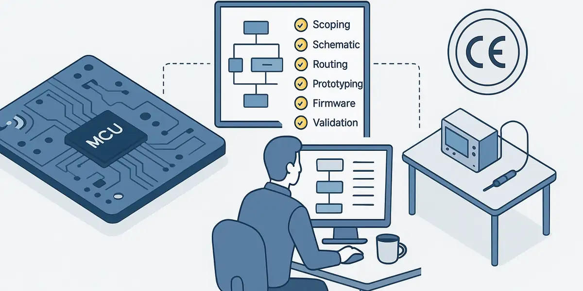
Time-to-market (TTM) for a connected product is the elapsed time between project kick-off and the first unit shipped to customers. Compressing it means parallelising hardware and firmware, picking pre-certified radio modules, anticipating CE/RED compliance and locking in supply alternates early. Q1 2026 benchmarks: 6 to 9 months consumer, 12 to 18 months industrial IoT, 24 to 36 months class IIa medical under ISO 13485 and IEC 62304.
Key takeaways
- Parallelising hardware, firmware and certification cuts TTM by 20 to 40 percent on the critical path.
- Pre-certified radio modules (Nordic nRF52, Silicon Labs BGM, u-blox) save 6 to 12 weeks of RED procedure under ETSI EN 300 328.
- ANSYS SI/PI simulation typically removes 1 to 2 PCB respins (6 to 10 weeks each).
- Documented BOM second sources aligned with IPC-2221 cut supply-chain risk by half.
- MVP scope in 4 to 6 weeks. Reserve the accredited CE/RED slot 8 weeks ahead.
In the connected-products market, shipping six months late often means a missed market window, a competitor planted ahead of you, or a funding round that closes without a working demo. TTM is not just a metric: it is frequently the deciding factor between commercial success and a stalled launch. At AESTECHNO, with more than ten years of practice in connected-product design, we have supported customers who absolutely had to hit hard deadlines: trade shows, fundraising milestones, seasonal launches. We have identified the levers that genuinely shorten a project without compromising quality or blowing up the budget. This guide walks through those proven methods.
Need to accelerate your IoT project? AESTECHNO expertise
We help companies cut their time-to-market by applying proven methods from the design phase onwards.
- Parallelisation of hardware, firmware and certification activities
- Use of pre-certified modules and proven reference designs
- Anticipation of supply-chain and certification risks
Contents
- Why time-to-market matters for connected products
- The real causes of delay in electronics projects
- Strategy 1: Parallelise activities
- Strategy 2: Use proven platforms and modules
- Strategy 3: Design for compliance from day one
- Strategy 4: Secure the supply chain upstream
- Strategy 5: Pick the right partners
- Strategy 6: Run iterative cycles
- Strategy 7: Pilot the schedule actively
- Comparison of acceleration strategies
- What does not work to accelerate
- Checklist: accelerate your IoT project
- Bottom line: five levers to prioritise
- FAQ: frequent questions on time-to-market
Why time-to-market matters for connected products
Time-to-market is the elapsed time between project kick-off and the first product unit shipped to customers, typically counted in months for connected hardware. For connected products this delay is especially critical because the market moves quickly: technologies, customer expectations and competitors all shift continuously. A perfect product delivered too late can already be obsolete on launch day. According to the GSMA 2025 IoT report, 14.7 billion connected devices were active worldwide in late 2025 and the median launch window keeps tightening quarter on quarter.
The stakes of a controlled time-to-market:
- Competitive advantage: being first on a segment captures customers before competitors do.
- Market windows: some launches are tied to events (trade shows, seasons, regulatory deadlines).
- Return on investment: the earlier the product ships, the earlier it generates revenue.
- Credibility: hitting your committed delivery dates strengthens trust with partners and investors.
Despite the pressure, accelerating does not mean cutting corners. A product launched with major defects or without certification will cost far more in returns, reworks and brand damage than a controlled delay would.
The real causes of delay in electronics projects
A delay in an electronics project is any deviation that pushes a milestone (PCB v1, EVT, DVT, PVT, certification, ramp) past its planned date. Delays in electronics development rarely come from one isolated cause. They are the cumulative result of technical, organisational and logistic factors that compound on each other. In our practice, we have observed the same delay patterns recurring across very different sectors. A principle from Ries (The Lean Startup) still applies: late iterations cost 10 to 100 times more when discovered during certification than when caught in design review. According to the Project Management Institute (PMI) 2025 Pulse of the Profession, 36 percent of complex hardware programmes slip beyond plan when the spec is not frozen before EVT.
Unstable specifications
The brief evolves during the project: new features requested, shifting priorities, late user feedback. Each major change after design starts can push the schedule by several weeks. A well-structured specification from day one limits this risk.
Underestimating complexity
IoT projects combine hardware, firmware, connectivity, cloud and a mobile app. Underestimating one of those bricks, or the interactions between them, drives surprises during integration. Bluetooth or LPWAN connectivity in particular tends to hide unforeseen difficulties.
Unplanned prototype iterations
Hoping for a fully functional prototype on the first try is unrealistic for a complex product. Failing to budget 2 to 3 iterations in the schedule mechanically leads to slippage.
Sourcing problems
One critical component out of stock or with a multi-month lead time can stall the entire project. The recent component shortages have made this reality painfully clear.
Certification failures
A product that fails CE/RED or EMC tests requires hardware fixes and a fresh round of measurements. Without anticipation, that easily means several weeks of delay.
Poorly managed external dependencies
Waiting for a customer decision, a deliverable from another vendor, or an internal sign-off that drags on. Idle time accumulates quickly when dependencies are not actively tracked and challenged.
Strategy 1: Parallelise activities
Parallelising activities means running tasks concurrently that are traditionally sequential, which compresses the overall project schedule. A documented lesson from Brooks (The Mythical Man-Month) still holds: interfaces must be frozen before branches can run in parallel. When they are, TTM contracts by 20 to 40 percent. The same discipline shows up in Kanban and Lean for hardware.
HW    : schematic -> PCB v1 -> PCB v2 -> industrialisation
FW    :   BSP     -> drivers -> app    -> validation
Radio :   eval    -> integ.  -> EMC pre-scan -> CE/RED
Supply:   BOM freeze -> long-lead orders -> pre-prod
// critical path = max(HW, FW, Radio, Supply)What can be parallelised
- Hardware and firmware: firmware development can start on an evaluation kit while the custom PCB is still being routed.
- Electronics and mechanics: the enclosure can be designed in parallel with the electronics if the interfaces are pinned down early.
- Design and procurement: long-lead components can be ordered as soon as the part choice is validated.
- Development and certification: EMC pre-scans can flag issues while the firmware is being finalised.
What must stay sequential
- Functional validation before the pre-series.
- Official certification testing on the final product.
- Industrialisation transfer once the design is signed off.
Risks of parallelisation
Parallelising creates risk: if an upstream decision changes, work done in parallel can be invalidated. The key is to parallelise only when interfaces are stable and the probability of change is low. Parallel work does not always save time: we have observed that premature parallelism on unstable interfaces ends up costing more than a slightly longer serial path.
Strategy 2: Use proven platforms and modules
Proven platforms are pre-certified modules and reference designs (BLE, LoRaWAN, NB-IoT) whose RF performance has been pre-characterised by the vendor. Building on these technology bricks, validated code libraries, reference SoMs and Yocto BSPs lets the team focus its development effort on the product's specific value-add. At AESTECHNO, we have observed that this approach significantly reduces technical risk while accelerating prototyping and certification. A Bluetooth module pre-certified to ETSI EN 300 328 (operating in the 2.4 GHz ISM band, +20 dBm conducted, 100 mW EIRP) typically saves 6 to 12 weeks of RED procedure. According to ETSI, modules already declared compliant under the FCC ID and CE-RED scheme can ship under a Declaration of Conformity (DoC) rather than the full radiated test campaign.
Pre-certified radio modules
Pre-certified Bluetooth, Wi-Fi or LoRaWAN modules avoid designing the RF stage from scratch and simplify certification. The unit-cost premium is largely offset by the gain in development time and the reduction in risk.
Development platforms
Starting from a reference platform (System on Module, extended evaluation board) rather than a 100 percent custom design lets you validate the concept quickly and reduce risk. Customisation can be limited to the strict minimum.
Reuse of code and designs
An experienced design firm capitalises on its past projects: validated component libraries, reusable functional blocks, firmware templates. This capitalisation accelerates each new project. We integrate proven blocks from previous engagements rather than reinventing them per project.
Integrated ecosystems
Some manufacturers offer complete ecosystems: hardware, SDK, connectivity stack, cloud tooling. Using these ecosystems reduces integration effort, at the price of increased vendor lock-in.
Strategy 3: Design for compliance from day one
Design for Compliance (DfC) is a methodology that builds CE/RED, FCC and EMC requirements into the schematic and PCB routing from the very first design review. Regulatory certification (CE, RED, FCC) is an incompressible milestone in any connected-product programme. Anticipating the standards' requirements as early as schematic capture and PCB routing avoids costly late-cycle iterations. In our practice, products designed with a Design-for-Compliance approach pass tests on the first attempt in the vast majority of cases. ESD and radiated emission requirements are tested during pre-scans, against IEC 61000-4-2 (8 kV contact, 15 kV air discharge) and CISPR 32 (Class B, 30 MHz to 6 GHz). According to NIST guidance on radiated emissions, an in-house pre-scan within 6 dB of the Class B limit is a strong predictor of first-pass success at the accredited lab.
Design for Compliance
Build EMC and RF best practice into the schematic and PCB from the start:
- Continuous ground plane, careful decoupling and a controlled stackup.
- Controlled impedance on high-speed traces: 50, 90 or 100 ohms depending on the bus.
- Differential pairs matched within plus or minus 5 mils of length skew.
- Filtering on external interfaces and via stitching around RF zones.
- Strict adherence to module integration guidelines (Nordic, Silicon Labs).
- Provisions for late tweaks (placeholder ferrites and capacitors).
These practices are detailed in our articles on RF PCB design and electromagnetic compatibility.
Systematic pre-tests
Running EMC and radio pre-tests before the official lab pass lets us catch and fix issues at much lower cost. This step adds a few days to the schedule, but it can save weeks by avoiding outright failures at the accredited lab.
Relationship with the lab
Reserve test slots early in the project. Accredited labs often have several weeks of waiting list. Waiting until the last minute to schedule tests is one of the most frequent causes of slippage we have observed.
Pre-manufacturing simulation: the strongest TTM accelerator
At AESTECHNO, we use ANSYS to simulate Signal Integrity (SI) and Power Integrity (PI), and to optimise antennas before fabrication. With these simulations we can tell, before fabricating, whether the board will operate, with good accuracy. This prediction targets the respin phase, where each PCB respin costs 6 to 10 weeks. Going from 2 respins to 0 means winning back an entire quarter.
Tektronix TekExpress in-house compliance lab
Our Tektronix oscilloscope runs the TekExpress compliance suite for PCI Express, USB 3.x, MIPI, DDR2/DDR3/DDR4, HDMI, Ethernet and LVDS. This in-house instrumentation lets us pre-qualify high-speed interfaces (eye diagram, jitter against the bus mask) before boards reach the accredited lab.
PCB designed by the book: a pre-production optimized prototype
Our signature: the design IS already a production design. We deliver a pre-production optimized working prototype on the first attempt: EMC pre-compliant, IPC-aligned and designed for high-volume manufacturing, not a "prototype to redo for production". This integrated pipeline (design, ANSYS simulation, validation, industrialisation) is the single largest TTM accelerator we bring to our customers.
Why choose AESTECHNO?
- 10+ years of expertise in connected-product design
- 100% success rate on CE/FCC certifications, across dozens of campaigns run over more than 10 years of practice
- 65 projects delivered since 2022
- French design firm based in Montpellier
- End-to-end support from concept to series production
Article written by Hugues Orgitello, electronics design engineer and founder of AESTECHNO. LinkedIn profile.
Strategy 4: Secure the supply chain upstream
Supply-chain hardening is the practice of identifying second sources, life-cycle status and lead times for every Bill of Materials (BoM) line at design time rather than at assembly. Proactive supply-chain management means anticipating sourcing risk during component selection, rather than absorbing it at assembly time. A part that is unavailable when assembly starts can stall a project for weeks or months, wiping out every gain achieved during design. According to the IPC association (ipc.org), an IPC-2221 compliant design with documented second sources cuts the supply-rupture risk by half. According to Bpifrance 2025 industrial sourcing analysis, French electronics startups that ordered long-lead MCUs at PCB v1 cut their median ramp delay by 40 percent compared to a freeze-then-order pattern.
Availability check
Before locking a component into the design, verify:
- Distributor stock levels.
- Lead time for replenishment.
- Life-cycle status (Active, NRND, EOL).
- Minimum Order Quantity (MOQ).
Second sources
For critical components, identify and validate alternates (second sources) at design time. If the primary part becomes unavailable, the project can carry on with the alternate without a respin.
Forward orders
Long-lead components (some microcontrollers, specialty connectors, RF parts) should be ordered as soon as their selection is validated, without waiting for the design to close. Excess-stock risk is generally lower than slip risk.
Strategy 5: Pick the right partners
A partner ecosystem is the network of design firm, PCB fabricator, EMS assembler and certification lab whose combined responsiveness sets the achievable cadence of an electronics programme. The choice of technical partners (electronic design company, PCB fabricator, EMS assembler, certification lab) directly drives the speed of execution on a project. An experienced and responsive partner anticipates problems, suggests proven solutions and delivers on schedule. At AESTECHNO, we have built a network of trusted partners that share our standard of responsiveness across France and Europe.
Design firm
An experienced design firm brings not only technical skills but also rehearsed processes, reusable designs and a working knowledge of the pitfalls to avoid. The time saved more than offsets the cost of expertise.
PCB fabricator
PCB fabricators offer different service tiers: standard (2 to 3 weeks), fast (1 week), express (a few days). The premium for fast service can be justified when holding a tight schedule.
EMS (assembly)
Working with a responsive and flexible EMS makes prototype-stage iteration faster. Geographic proximity (Europe vs Asia) often makes the difference for small batches and prototypes.
Certification lab
Building a relationship with a lab that already knows your products speeds up testing: less explanation time, better anticipation of likely issues.
Strategy 6: Run iterative cycles
Iterative hardware development is a lean-hardware approach that progressively validates critical functions through short EVT, DVT and PVT cycles rather than aiming for a perfect design on the first iteration. This Minimum Viable Product (MVP) method, documented in Ries (The Lean Startup), reduces risk and can paradoxically accelerate the project by surfacing problems as early as possible. On an IoT product running a Real-Time Operating System (RTOS) such as Zephyr or FreeRTOS, a typical iterative cycle runs 4 to 6 weeks between two prototypes, with current draw measured down to the µA range in deep-sleep and Mbps throughput characterised at the BLE radio.
Hardware MVP
Define a hardware Minimum Viable Product: which functions are strictly required for a first version? Secondary features can be deferred to a later release.
Rapid prototyping
Validate the critical concepts as early as possible with simple prototypes (evaluation kits, mock-ups, proof of concepts) before committing to a full design. A POC built in a few weeks can prevent months of work in the wrong direction.
Early feedback
Get prototypes into the hands of users or customers as early as possible. Early feedback lets you adjust the product before it is too late to change direction.
Strategy 7: Pilot the schedule actively
Active schedule piloting is a project-management discipline that tracks real progress against the plan on a weekly cadence and triggers corrective actions before delays compound. A frozen plan that is never updated quickly becomes fiction. Only regular tracking keeps the project on the rails. According to the PMI PMBOK Guide 7th edition, programmes that update the critical path weekly close 22 percent more milestones on time than those reviewed monthly.
Identify the critical path
The critical path is the sequence of activities that drives the minimum project duration. Any slip on the critical path delays the project. Concentrate effort and oversight on those activities.
Regular progress checkpoints
Short weekly stand-ups let problems surface before they turn critical. Each contributor must escalate risks and blockers without waiting for the next milestone.
Risk management
Identify potential risks at project start and define mitigation plans. An anticipated risk is a manageable risk. A risk discovered late is a crisis. Our guide on risk management in electronics projects details this methodology.
Fast decisions
Idle time waiting on decisions piles up fast. Establish a clear decision process and empower stakeholders to call the shot quickly.
Comparison of acceleration strategies
Comparing TTM strategies means quantifying the time saved, the risk taken and the cost incurred. Each strategy acts on a phase and produces a measurable gain in weeks. According to the French ANSSI cybersecurity agency, anticipating compliance audits also reduces certification lead time by around 25 percent for connected products.
Each acceleration strategy carries a different ratio between potential time savings, implementation complexity and associated risk. The table below summarises these criteria to help prioritise the levers best suited to your situation.
| Strategy | Potential gain | Complexity | Risk | When to apply |
|---|---|---|---|---|
| Parallelisation | High | High | Medium | Stable interfaces and experienced team |
| Pre-certified modules | High | Low | Low | Products with radio connectivity |
| Compliance anticipation | High | Medium | Low | Every certified product |
| Supply-chain hardening | Medium | Low | Low | Specific or long-lead parts |
| Right partners | Medium | Low | Low | New project or vendor change |
| Iterative approach | Medium | Medium | Low | Innovative products with high uncertainty |
| Active piloting | Medium | Low | Low | Every schedule-constrained project |
What does not work to accelerate
A TTM anti-pattern is a practice that promises time savings but actually drags the project out. According to the PMI in its PMBOK Guide, the recurring traps are: late staffing surge, skipping EMC pre-scans and removing interface reviews. Despite their intuitive appeal, these shortcuts produce the opposite effect.
Some popular shortcuts intuitively seem to accelerate a project but in practice produce the inverse outcome. We have observed that these false good ideas are responsible for many schedule slippages, because they introduce problems that surface late and cost more to fix than they ever could have saved.
Skipping validation steps
Cutting pre-tests, reducing functional testing, skipping the pre-series. These time savings get paid back in late-discovered defects that are far more expensive to fix.
Compressing the schedule unrealistically
Demanding an "aggressive" timeline without changing method or resources. Pressure does not create time. It creates stress, mistakes and turnover.
Adding people late
Adding engineers to a late project usually slows it down further (Brooks's law). Coordination consumes time and new joiners need a learning curve before contributing.
Changing scope mid-flight
Adding features "while we're at it" during development. Each addition pushes delivery and increases risk.
Checklist: accelerate your IoT project
A Time-to-Market (TTM) checklist is a milestone-gate verification list that locks BoM freeze, documented second sources, internal EMC pre-scan and frozen HW/FW interfaces before any branch goes parallel. As ENISA underlines in its 2025 IoT baseline, this checklist must also cover cybersecurity per ETSI EN 303 645 and IEC 62443: ATECC608B secure element, MCUboot signed bootloader and a CycloneDX SBOM (Software Bill of Materials) shipped with every firmware release. According to ANSSI, weaving these controls into the design phase rather than retrofitting them at certification cuts the audit cycle by around 25 percent for connected products in 2026.
This checklist groups the concrete actions to verify at every phase of your project to maximise the chances of holding the schedule. It synthesises the best practices laid out in the strategies above and works as a project-review crib sheet.
Preparation
- Specification stabilised and signed off by every stakeholder.
- Features prioritised (must-have vs nice-to-have, MoSCoW method).
- Technical risks identified and mitigation plans defined.
- Realistic schedule with buffer for the unexpected.
Design
- Pre-certified modules used where relevant.
- Component availability verified.
- Second sources identified for critical parts.
- EMC and certification constraints integrated from schematic capture.
Execution
- Activities parallelised wherever interfaces are stable.
- Long-lead components ordered ahead of design freeze.
- Lab slots reserved early.
- Regular progress checkpoints scheduled.
Partners
- Responsive and experienced electronic design company.
- PCB fabricator with a fast service available.
- Flexible EMS for prototypes.
- Fast internal decision process.
Bottom line
To compress the TTM of a connected product without sacrificing quality, here are the five levers we recommend activating in sequence:
- TTM benchmarks: 6 to 9 months for a consumer device, 12 to 18 months for industrial IoT, 24 to 36 months for a class IIa medical device under ISO 13485 and IEC 62304.
- Hardware / firmware parallelisation: start firmware on an evaluation kit while PCB routing is still in progress. Typical gain: 20 to 40 percent on the critical path.
- Pre-certified radio modules: a Bluetooth or LoRaWAN module compliant with ETSI EN 300 328 saves 6 to 12 weeks of RED procedure compared to a from-scratch RF design.
- Internal EMC pre-scan: per CISPR 32 and IEC 61000-4-2, a pre-scan run before the accredited lab pass saves 4 to 8 weeks per failed iteration avoided.
- Pre-fabrication SI/PI simulation: an ANSYS simulation flags impedance and integrity violations before respin. Each PCB respin costs 6 to 10 weeks.
These levers do not replace validation. They compress the sequence without skipping steps.
Your IoT project on a tight schedule? AESTECHNO expertise
From a blank sheet to a certified, production-ready product, we support every milestone with TTM compression in mind:
- Hardware / firmware parallelisation from day one
- Pre-certified radio modules and proven reference designs
- In-house EMC pre-scan and TekExpress compliance testing
- Industrialisation and series ramp-up
FAQ: frequent questions on time-to-market
What is a realistic schedule for an IoT product?
For a moderately complex IoT product (microcontroller, BLE or LoRa connectivity, a handful of sensors), expect 10 to 15 months from concept to series production. That includes proof-of-concept, 2 to 3 prototype iterations, pre-series and certification. Simpler products can close in 6 to 8 months. Complex products take 18 months or more.
How do I trade off speed against quality?
Speed and quality are not necessarily opposed. The methods that genuinely accelerate (parallelisation, reuse, anticipation) do not hurt quality. What does hurt quality is skipping validation steps or operating in permanent crisis mode. A poor-quality product launched fast costs more in returns and brand damage than a slightly delayed, solid one.
Can a project that is already late be rescued?
Yes, but options are limited. We can parallelise the remaining activities, mobilise extra resources on the critical path, or trim the scope (defer features). Adding people to a late project usually does not help. The best strategy is to anticipate slippage and act early.
Do agile methods apply to hardware?
Partially. Agile principles (short iterations, fast feedback, adaptation) apply to hardware via rapid prototyping and the MVP approach. Hardware does have constraints software does not: fabricating a PCB takes time, modifications cost real money, and certification is an incompressible milestone. Agility in hardware is constrained agility.
How do I convince leadership to invest in going faster?
Quantify the cost of delay: lost revenue, missed market window, advantage handed to competitors. Compare that cost to the proposed investment (fast PCB service, extra headcount, pre-certified modules). In most cases, the ROI on acceleration is positive when TTM is genuinely critical.
Should I in-source or outsource to go faster?
Outsourcing to a specialised product development partner usually starts faster (no recruitment) and gives immediate access to experienced engineers. For a one-off project on a tight schedule, that is often the right move. In-sourcing takes time to set up but can be more reactive over the long term. See also our DFM guide for the related production-cost angle.
Related articles
- Electronic design services methodology: AESTECHNO 6-step EVT/DVT/PVT process from spec to pre-series.
- Electronic product specification guide: how to write a brief that gets shipped.
- CE/RED certification for IoT products: process and lead times.
- Design for Manufacturing: cost-cutting playbook for electronic products.
- PCB design: stack-up, impedance, EMC: routing techniques aligned with IPC.
- Electromagnetic compatibility (EMC): pre-scans and lab-pass strategies.
- Industrial IoT cybersecurity: CRA and ETSI EN 303 645 alignment.