23 min read Hugues Orgitello EN
How a PCB works: an illustrated guide for engineers and product managers
How a PCB works explained step by step: FR4 substrate, copper layers, fabrication and assembly. Illustrated guide by AESTECHNO Montpellier.
A Printed Circuit Board (PCB) is a rigid plate that serves as both a mechanical support and an electrical interconnection network for the components of an electronic device. This illustrated guide explains how a PCB works, from raw copper-clad laminate to a tested, populated board. At AESTECHNO in Montpellier, we have been designing PCBs from 2 to 28 layers for over 10 years, in line with IPC standards: IPC-2221, IPC-2222, IPC-6012 and IPC-7351.
Bottom line
- A PCB stacks four functional layers: Flame Retardant 4 (FR4) substrate, copper layers (35 µm or 1 oz/ft² standard), solder mask, and silkscreen. High-performance materials come from Rogers (RO4350B, Dk 3.48) or Isola (I-Tera MT40) for RF and high-speed work.
- Layers vs use case: 2 layers for Arduino-class IoT sensors, 4 layers for MCU + RF, 6 to 8 layers for SoC + DDR, 10 to 12 layers for FPGA + LPDDR4, and 14 to 28 layers in High Density Interconnect (HDI) for servers and embedded AI.
- Key acronyms: Design for Manufacturing (DFM), Design for Assembly (DFA), Design for Test (DFT), Signal Integrity (SI), Power Integrity (PI), Electromagnetic Compatibility (EMC), Via-in-Pad (VIP), Hot Air Solder Leveling (HASL), Electroless Nickel Immersion Gold (ENIG), Ball Grid Array (BGA).
- Mandatory IPC standards: IPC-2221 (generic design rules), IPC-2222 (rigid boards), IPC-6012 (rigid qualification, classes 1 / 2 / 3), IPC-7351 (footprints), IPC-A-600 (visual acceptability), IPC-A-610 (assembly acceptability), IPC-4761 (protected vias).
- Typical thresholds: minimum trace 100 µm (4 mil) standard, 75 µm (3 mil) HDI, 100 µm laser microvias, differential impedance 90 Ω (USB) or 100 Ω (Ethernet) within ±10%.
PCBs are everywhere, in your phone, your car, your coffee machine, your office badge, yet most people have no idea how they are made. This guide explains, step by step, how one works, from raw copper-clad laminate to an assembled and tested board. No electronics degree required: if you accept that a wire conducts current and a switch breaks it, you have the prerequisites. At AESTECHNO we have been designing PCBs for industrial, IoT, medical and embedded applications for more than 10 years, up to 28 layers, in HDI and rigid-flex.
Need to design a PCB for your project?
We support project owners and industrial OEMs across the full PCB design path, from schematic to fabrication-ready files:
- Design from 2 to 28 layers, prototype to series production
- High-density routing, signal-integrity management
- Gerber deliverables ready for fabrication and assembly
Contents
- What is a PCB?
- How many layers does your PCB need?
- From schematic to routing: the design flow
- Electronic components on a PCB
- How is a PCB fabricated?
- How are components assembled?
- Tests and quality control
- Common PCB design mistakes to avoid
- AESTECHNO PCB expertise
- Bottom line
- FAQ
What is a printed circuit board?
A printed circuit board, or PCB, is a rigid plate that provides both mechanical support and an electrical interconnection network for the components of an electronic device. According to the IPC (the industry reference body), IPC-2221 defines the generic design rules, IPC-6012 defines the qualification classes for rigid boards, and IPC-7351 standardises SMD footprints. The PCB is the skeleton and the nervous system of every electronic device.
To picture a PCB, imagine a city seen from above. The electronic components, resistors, capacitors, processors, are the buildings. The copper traces etched on the board are the streets and motorways linking these buildings together. The substrate (the plate itself) is the ground on which everything sits. And just like in a city, there is a precise master plan: each road has a calculated width, each junction is engineered, and nothing is left to chance.
A PCB stacks several layers, each with a specific role:
- The substrate (FR4): the foundation. FR4 (Flame Retardant 4) is a fibreglass + epoxy composite that is rigid, insulating and heat-resistant. It plays the role of the "ground" on which everything is built. For RF or high-speed applications, we swap FR4 for Rogers (Rogers RO4350B, Dk 3.48) or Isola materials (Isola I-Tera MT40) whose dielectric stability is far higher.
- The copper layers: the "roads" for electrons. Copper is laminated (pressure-bonded) onto the substrate, then chemically etched to leave only the required traces. Standard thickness is 35 µm (1 oz/ft²), and can be increased for higher current.
- The solder mask: this green layer (or blue, red, black, the colour is an aesthetic choice) covers the copper to protect it from oxidation and to prevent shorts during soldering. It is opened only at the pads where components must be soldered.
- The silkscreen: the white ink layer printed on top of the solder mask. It carries reference designators (R1, C5, U3), logos and polarity marks. It is the "map" technicians use to find their way on the board.
To stay with the city analogy: FR4 is the ground, the copper traces are the roads, the solder mask is the protective coating that prevents erosion, and the silkscreen is the road signage. Together they form a coherent, complete system.
How many layers does your PCB need?
The copper-layer count of a PCB is the single decision that drives interconnect complexity, board size and cost. According to IPC-2221 and as cited by IEEE 802.3 channel guidance, three broad categories exist: single-sided, double-sided, and multilayer. The right choice depends on component density, maximum signal frequency, and budget.
| Layer count | Complexity | Typical use | Relative cost |
|---|---|---|---|
| 1 layer (single-sided) | Very simple | Toys, remotes, basic PSUs | Very low |
| 2 layers (double-sided) | Simple | Arduino-class boards, small IoT sensors | Low |
| 4 layers | Intermediate | MCU + sensors + connectivity, dedicated ground plane | Moderate |
| 6 to 8 layers | Advanced | SoC with DDR, high-speed interfaces (USB 3, PCIe Gen 3) | Moderate to high |
| 10 to 12 layers | Complex | Dense FPGAs, multi-core processors, LPDDR4 | High |
| 14 to 28 layers (HDI) | Very complex | Servers, embedded AI, PCIe Gen 5, high-density modules | Very high |
At AESTECHNO we have designed across this full range, from entry-level 2-layer boards to 28-layer HDI stack-ups (laser microvias, buried vias) for industrial and embedded-AI applications. Each rung carries its own trade-offs.
Contrary to the intuition that more layers always means better routing, in our practice we have observed that a well-thought-out 4-layer board can carry faster signals than a poorly arbitrated 8-layer one. The continuity of reference planes, as IPC-2152 underlines in its current-carrying capacity guides, weighs more than the raw layer count. We recommend specifying the layer count from the loss budget and the BGA pitch, not from a default rule of thumb.
Single, double-sided and multilayer
Single-sided (1 layer) carries copper on one side only and is reserved for the simplest products (remotes, basic PSUs). Double-sided (2 layers) adds copper on both faces with plated through-hole vias bridging them, the workhorse of Arduino-class boards and simple industrial controllers. Multilayer (4, 6, 8, 12+) stacks copper layers separated by insulating substrate, with inner layers used as power and ground planes while outer layers carry accessible signals. Multilayer is mandatory for modern processors, high-speed memory and RF circuits. For stack-up optimisation, see our piece on PCB stack-up, controlled impedance and EMC.
At AESTECHNO we have designed stack-ups up to 28 layers, a level rarely reached on the French market, with hands-on HDI (laser µVias, buried vias), flex, rigid-flex, integrated PCB antennas, and harsh-environment work (RF, high-speed, high vibration, temperature extremes).
From schematic to routing: the design flow
PCB design is a four-step structured process (schematic, netlist, placement, routing) that turns an idea into a fabrication file. According to Altium and as noted by Siemens in its Xpedition documentation, the flow is iterative and demands a design review at every step. Understanding it lets you talk shop with your design house. In our practice, we have observed that teams skipping the placement review burn three weeks of routing rework on average.
The four steps
Schematic capture draws the circuit in an EDA tool (Altium Designer, KiCad, Cadence) by placing component symbols and the logical connections between them. At this stage we define the function, not the geometry. Netlist extraction turns the schematic into an exhaustive list of every connection between pins, the language the layout tool can act on. Component placement arranges parts physically on the board, a 3D puzzle balancing mechanical, thermal, electrical and manufacturing constraints. Placement is often the step demanding most experience: good placement makes routing simple, bad placement makes it impossible. Trace routing draws the copper paths that realise the netlist, each trace width set by current and required impedance, and respecting DFM rules and EMC constraints. The flow loops; it is normal to walk back to the schematic to fix an oversight, or to revisit placement to unlock a routing problem.
Our toolchain in practice. We use Altium Designer for demanding industrial work (multi-variant management, multi-user review, library management) and KiCad where the open-source ecosystem brings a real advantage. For SI/PI simulation and dense routing we use Ansys HyperLynx and Polar tools for impedance computation. We export Gerbers in RS-274X or IPC-2581 (the modern open exchange format backed by Altium, Cadence and Siemens), accompanied by an IPC-aligned master drawing on complex boards. Altium and KiCad have different philosophies; the right pick depends on project context, not personal taste.
Electronic components on a PCB
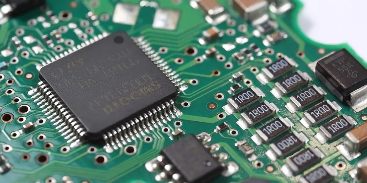
Components are the "inhabitants" of our city-PCB. They perform the actual circuit functions: filter, amplify, convert, compute, communicate. According to JEDEC, the standards body for semiconductor packages, and as cited by IEEE packaging working groups, components fall into two main families: through-hole and surface-mount (SMD). Modern packages include Ball Grid Array (BGA), Quad Flat Package (QFP), Quad Flat No-lead (QFN) and Chip Scale Package (CSP).
Through-hole vs SMD
Through-hole components have leads that pass through drilled holes and are soldered on the opposite side, the historic technology. They still have a place for connectors (mechanical stress), power components (heat dissipation), and hand-built prototypes. SMD parts are soldered directly to the surface, without piercing the substrate. A 0402 SMD resistor measures 1.0 by 0.5 mm, barely visible to the naked eye. Miniaturisation lets us pack more parts on a given area and shorten distances, improving high-frequency performance.
Common SMD sizes (four-digit code, dimensions in hundredths of an inch): 0805 (2.0 by 1.25 mm) easy to hand-solder, 0603 (1.6 by 0.8 mm) industry workhorse, 0402 (1.0 by 0.5 mm) high-volume production, 0201 (0.6 by 0.3 mm) for smartphones and wearables. Size is a trade-off: smaller parts shrink the board and cut unit cost in volume, but demand more accurate placement, finer stencils, tighter solder profile control. Beyond passives, a PCB carries ICs in QFP, BGA (solder balls under the body, forcing multilayer routing) and QFN packages.
How is a PCB fabricated?
PCB fabrication is a sequence of chemical, mechanical and optical steps (etching, drilling, plating, masking, silkscreening, finishing) that turns raw copper-clad laminate into a board ready to assemble. Final accuracy depends on stack-up quality, interlayer registration and drill tolerance (±50 µm typical). According to IPC-6012, these tolerances are codified per class. As noted by Panasonic in its FR4 process sheets, going below ±25 µm registration requires HDI-grade equipment that not every fab carries.
Gerber files, etching, drilling
The industry-standard fabrication format is Gerber. A Gerber set carries a 2D image of every layer (front and back copper, front and back mask, silkscreen, drill); the fab uses it as a build plan. Copper etching starts from a substrate fully clad with copper: photoresist is applied, exposed to UV through a mask, then unprotected copper is dissolved in a chemical bath. Only the traces and pads remain. Drilling uses very small bits (down to 0.1 mm for microvias) at up to 150,000 rpm; the hole walls are then plated (electroless then electrolytic copper) to create interlayer continuity.
Mask, silkscreen, surface finish
The solder mask covers everything except the solder pads. The silkscreen is purely informational, screen- or inkjet-printed reference designators that let a technician find C47 on the board. The surface finish protects exposed pads from oxidation. The two most common are:
- HASL (Hot Air Solder Leveling): the board is dipped in molten tin, then the excess is blown off with hot air. Cheap and tough, but the surface is not perfectly flat, which can be a problem for very fine-pitch parts (BGA, QFN). Per IPC-4552, typical thickness is 1 to 40 µm.
- ENIG (Electroless Nickel Immersion Gold): a nickel layer (3 to 6 µm) followed by a gold layer (0.05 to 0.10 µm) is chemically deposited on the pads (IPC-4552). Perfectly flat surface, excellent solderability, long shelf life (12 months). More expensive, but indispensable for fine-pitch parts and boards stored for a long time before assembly.
Other finishes exist (OSP, immersion tin, immersion silver), each with its own trade-offs.
The IPC standards family
The IPC standards are the international corpus that codifies PCB design, qualification and acceptability, maintained by the IPC (Institute for Printed Circuits, Illinois, USA). The ones we cite most often:
- IPC-2221, generic PCB design rules (trace widths, tolerances, stack-ups).
- IPC-2222, rigid-board-specific design, supplements IPC-2221.
- IPC-2581, open digital exchange format (modern alternative to Gerber) backed by Altium, Cadence and Siemens.
- IPC-4761, protected-via specification (Via-in-Pad, tented, capped, filled).
- IPC-6012, qualification and performance of rigid PCBs. Defines classes 1 / 2 / 3, respectively consumer, industrial, high reliability (medical, aerospace).
- IPC-A-600, visual acceptability criteria for PCBs (surface, holes, traces).
- IPC-A-610, assembly acceptability criteria (joint quality, component alignment).
- IPC-7351, footprint standards for SMD parts.
Contrary to the widespread idea that IPC is just paperwork, these standards encode decades of industrial field feedback. Ignoring IPC-6012 Class 2 on an industrial-environment product is a fast track to field failures. At AESTECHNO we systematically align our technical files with the right IPC class for the product, and we call out the required class in the master drawing handed to the fab.
How are components assembled?
Assembly is the step where a bare PCB is populated with its components, either by hand or by automated pick-and-place plus reflow. According to IPC-A-610 Class 2 or Class 3, acceptability criteria differ (geometric tolerances, joint quality). At volume, the process pick depends on component types (through-hole or SMD) and the throughput target.
The four steps
Solder paste printing lays a thin layer of paste (micro-sized tin alloy spheres in flux) on the pads through a stainless-steel stencil. Too much paste shorts; too little gives dry joints. Pick-and-place robots, vacuum-nozzled and vision-aligned, lay parts on the tacky paste at up to 80,000 components per hour with 25 µm accuracy. Reflow soldering sends the populated board through an oven that follows a precise profile: preheat, ramp, peak (230 to 250 °C for lead-free alloys), controlled cooldown. Wave soldering handles through-hole parts: the underside passes over a wave of molten tin that wets leads and plated holes. Hand soldering remains relevant for prototypes and very small series, manageable down to 0603 with the right tools.
Tests and quality control
Post-assembly tests are the controls that separate a "maybe-functional" board from a compliant one, via AOI, X-ray, In-Circuit Test and functional test. According to Keysight and as noted by the IEEE Test Conference, a defect that escapes detection before integration costs 10 to 100 times more to fix later, which justifies the investment in automated benches as soon as pre-series. According to IEC 61191 (soldering acceptance criteria), the same logic applies upstream of the test bench, on the reflow profile itself.
The four test layers
AOI (Automated Optical Inspection) photographs each face of the board with high-resolution cameras and compares against a reference model. It catches missing parts, offsets, reversed polarity, insufficient solder, visible shorts. Fast and non-invasive, it sits at end-of-line. X-ray inspection handles parts whose joints are hidden, BGAs above all, by "seeing through" the body to verify solder balls: voids, alignment, shorts. ICT (In-Circuit Test) uses a bed-of-nails fixture studded with test pins that contact precise points, electrically checking every component value and connection. Exhaustive, but it demands a board-specific fixture. Functional test powers the board, loads firmware and exercises I/O, the test closest to real-world conditions.
Lab practice: measurements and audits
Contrary to the assumption that a generic 100 MHz scope captures everything, in our lab we have observed that it masks transients decisive for the energy budget. We run our test bench around precision instruments matched to each measurement class. To characterise ultra-low standby currents (battery-powered IoT), we combine a Nordic PPK2 dynamic profiler and a Tektronix Keithley DMM7510 7.5-digit DMM that descends to picoampere territory, the precision needed to validate multi-year autonomy claims. On a recent project we measured 180 nA standby on a BLE sensor node powered by a CR2032 cell.
For high-speed digital buses (DDR, PCIe, USB 3.x, HDMI, LVDS), we have audited many client buses with eye diagrams, with sometimes counter-intuitive results. Some boards pass with margin to spare. Others reveal insufficient margins, invisible at nominal operation but fatal at series ramp-up. We rely on a Tektronix oscilloscope equipped with the TekExpress compliance suite, which lets us close the loop between routing, eye-diagram measurement and stack-up adjustment in-house. We measured, on a recent client project, a 35% vertical eye-opening drop between two FR4 batches from different lots, against a PCIe Gen 3 mask defined by IEEE-aligned PCI-SIG specs. Despite a clean DRC, we recommend automated TekExpress runs against the SerDes mask before fabrication release. In our practice, this catches one in five layouts that would otherwise eat a respin cycle. Contrary to the assumption that an eye-diagram audit is reserved for 10 Gbps and above, in our lab we observed measurable closure on PCIe Gen 2 (5 Gbps) DDR4-1600 (1.6 GHz effective) on poorly stacked 4-layer boards.
Common PCB design mistakes to avoid
PCB design mistakes are the recurring traps that cost full respins when they slip past fabrication. According to IPC-A-600 visual acceptance and IPC-A-610 assembly criteria, the same defect families recur project after project. Knowing them before starting your first design saves time, money and a lot of frustration. Here are the ones we see most often.
In our practice, we have constructed a measurement-based protocol to characterise these defects: we measured, on a recent client project, three independent failure modes on a single ground-plane fragmentation. According to the test procedure aligned with IPC-A-610 Class 2, each one would have escaped a generic functional test. Despite the board passing 100% AOI, the field-return rate stayed above the customer threshold. Contrary to the idea that AOI catches everything visible, our recent client project revealed that hidden BGA voids represent the dominant blind spot. The countermeasure: 100% X-ray inspection on the critical BGA references during NPI ramp-up.
The five recurring traps
Wrong footprint. Mistake number one. The schematic part does not match the real footprint, pads too close, too far, wrong order, and the board has to be re-spun. Systematic verification against the datasheet is non-negotiable. Decoupling caps missing or misplaced. A cap forgotten or sat 2 cm from its IC behaves like a shock absorber not bolted to the wheel. We have measured a 4 dB difference in radiated emissions between a 1 mm decoupling and a 4 mm decoupling on the Vdd pin of an MCU clocked at 168 MHz. Fragmented ground plane. A plane cut by traces, holes or slots creates parasitic loops and degrades signal quality. Thermal relief misunderstood. Without spokes, the plane drains heat away from the soldering iron before the joint melts. Beginners sometimes delete the reliefs to "improve conductivity", a counter-productive call. Ignoring DFM rules. Every fab has its own capability envelope; designing outside it draws a building no one can build. DFM is a hard requirement, not an option.
Real lab cases
Three concrete examples we have seen when taking over client designs, real cases that show why mistakes are rarely visible in simulation or even in prototype, and only show up in series production or in the field:
- Case 1: fragmented ground plane on an IoT product. The main GND plane was cut by several power traces, creating a return loop that only manifested at high temperature. Contrary to intuition, the issue was not on the signal trace but on the return path. We systematically recommend routing power on a dedicated layer as soon as the board reaches 4 layers.
- Case 2: thermal reliefs deleted on a power board. A client had stripped reliefs thinking it would help conductivity. Result: impossible to hand-solder in prototype, and in series, dry joints invisible to AOI but caught at functional test. Rather than delete reliefs, we recommend sizing the pad and the via count for the expected current. That is engineering.
- Case 3: IPC-6012 Class 2 ignored. An industrial-design takeover sourced in Asia without IPC class spec, where the vias had a 10:1 aspect ratio (too high), causing plating fractures after thermal cycling. In our practice, we explicitly require IPC-6012 Class 2 minimum in the master drawing for any industrial product, and Class 3 for medical and aerospace.
AESTECHNO PCB expertise
We design PCBs from 2 to 28 layers for industrial, medical, IoT and embedded applications, including HDI, flex and rigid-flex form factors, and integrated PCB antennas. Our signature: the design is already a production design, EMC-pre-compliant, IPC-aligned, ready for high-volume manufacturing. We have observed that the most successful projects are the ones where the design house and the customer speak the same language, the very goal of this guide.
- Manufacturing-first design: DFM rules applied from component placement, not at the end of the project.
- Signal-integrity ownership: calculated stack-up, controlled impedances, continuous ground planes, the fundamentals of high-speed routing.
- Full documentation: annotated schematics, validated Gerbers, verified BOM, master drawing for complex boards.
- Industrialisation support: we follow the board through prototype validation and into series production.
Whether you are kicking off a project, improving an existing board, or industrialising a product, our electronic design house in Montpellier is here to help.
Why choose AESTECHNO for your PCBs?
- 10+ years of expertise in multilayer PCB design
- 100% success rate on CE/FCC certifications
- 65 projects delivered since 2022
- French design house based in Montpellier, responsive and accessible
- IPC, DFM, EMC standards mastered, from prototype through series
Article written by Hugues Orgitello, electronic design engineer and founder of AESTECHNO. LinkedIn profile.
Have a PCB project in mind?
Get in touch for a free first call. We will look at your need and propose a fitting approach, from a simple 2-layer PCB to a high-density multilayer board.
Bottom line: the key points of a PCB
A PCB is not just a copper plate: it is the element that conditions the reliability, performance and production cost of an electronic device. The points to take away from this guide:
- A PCB combines four essential layers: substrate (FR4), etched copper, solder mask, silkscreen. Each has a precise role.
- Layer count follows circuit complexity, from 1 layer for toys to 28 layers for embedded AI or PCIe Gen 5 buses.
- The design flow is schematic to routing to Gerber to fabrication to assembly to test. Every step has its own constraints.
- DFM is not optional: design within the fab's capabilities, not the other way round.
- EMC and IPC compliance start at the schematic, not at the end when it is too late.
To go further, see our companion piece on PCB design: stack-up, impedance and EMC or our deep-dive on electromagnetic compatibility. For the wider design context, consult our methodology overview.
FAQ: printed circuit boards
What is the difference between a PCB and a PCBA?
A PCB (Printed Circuit Board) is the bare board, the substrate with its copper traces, solder mask and silkscreen, but without components. A PCBA (Printed Circuit Board Assembly) is the same board after the components have been soldered. The PCB is the support; the PCBA is the functional product.
Why are most PCBs green?
The green colour comes from the solder mask. Green was the historic colour, the easiest to produce and the most contrasted for visual inspection. Today fabs offer blue, red, black, white and other colours. The choice is mostly aesthetic, although green stays the most common and often the cheapest because the process is the most mature.
How many layers do I need for my project?
It depends on circuit complexity. A simple circuit (microcontroller, a few sensors) fits on 2 layers. A circuit with a processor, memory and multiple interfaces typically needs 4 to 6 layers. High-speed, RF or very dense circuits can demand 8, 10 or 12+ layers, up to 28 layers for embedded AI and PCIe Gen 5. Layer count drives fabrication cost directly, so it is important not to over-spec.
Can a PCB be made at home?
Yes, for simple prototypes. Makers fabricate single- or double-sided PCBs with craft methods: toner transfer, ferric chloride etch, manual drilling. Quality and reproducibility are limited though. For any project headed to series production or carrying fine-pitch parts (BGA, 0402), professional fabrication is required. Rapid-prototyping services with a few-day lead time make home fabrication harder to justify.
How long does a PCB last?
A correctly designed, fabricated and protected PCB can last decades. Lifetime depends on operating environment (temperature, humidity, vibration), material quality and surface finish. Automotive and aerospace PCBs target 15 to 30 years. The main degradation drivers are corrosion (humidity), thermal fatigue (temperature cycles) and mechanical stress (vibration).
What is the difference between a through-hole via and a microvia?
A through-hole via is a plated hole that crosses every layer of the PCB, top to bottom. A microvia is a very small via (typically 0.1 mm) that connects only two adjacent layers, drilled by laser instead of mechanical bit. At AESTECHNO we routinely use laser microvias and buried vias on HDI designs up to 28 layers, mandatory under fine-pitch BGAs and on density-critical products.
Related Articles
- PCB design: stack-up, impedance and EMC, the rigorous companion to this guide
- Design for Manufacturing in electronics, designing for manufacturability
- High-speed PCB design, signal integrity and advanced routing
- Electromagnetic compatibility (EMC), standards and best practices
- AESTECHNO electronic design house, our methodology and services