Concevoir l’électronique pour réussir dans l’IoT en 2026 : Comment garder une longueur d’avance
Introduction :
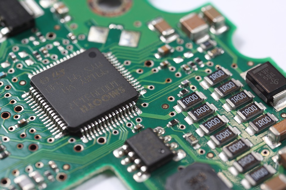
L’Internet des objets (IoT) transforme tous les secteurs – de l’usine connectée à l’agriculture intelligente. Mais derrière chaque bon produit IoT, il y a une carte électronique bien conçue, fiable, et optimisée pour le terrain.
Chez AESTECHNO, nous accompagnons les entreprises dans la conception de cartes électroniques sur mesure pour l’IoT – performantes, robustes et prêtes à être déployées.
Pourquoi les cartes standards ne suffisent plus
Aujourd’hui, l’IoT industriel ne peut pas se contenter de cartes électroniques génériques. Pour passer du prototype à une solution fiable et certifiée, la conception sur mesure est indispensable :
✅ Résister aux environnements extrêmes – Poussière, humidité, vibrations, perturbations électromagnétiques ? Nos designs sont prêts.
✅ Fonctionner pendant des années sur batterie – Microcontrôleurs basse consommation, gestion intelligente du sommeil, régulateurs efficaces.
✅ Communiquer sans faille – LoRa, LTE-M, Wi-Fi, Zigbee, Bluetooth, RS485… Nous les avons tous intégrés.
✅ Réussir la certification du premier coup – La conformité CEM et CE est intégrée dès la conception.
3 problèmes concrets que nous avons résolus grâce à une conception intelligente
🔹 Surveillance de la chaîne du froid (Agroalimentaire)
Capteurs LoRa à batterie avec une précision de ±0,2 °C – déployés dans des camions frigorifiques en Europe.
🔹 Irrigation intelligente (Agritech)
Cartes électroniques basse consommation avec BLE + recharge solaire, mises à jour à distance dans des vignobles.
🔹 Suivi d’équipements industriels (Industrie 4.0)
PCB sur mesure intégrant BLE Mesh + Modbus pour la géolocalisation temps réel dans un site de production lourd.
Pourquoi les entreprises choisissent AESTECHNO pour leurs projets IoT
🧠 Nous anticipons les problèmes – Nos conceptions prennent en compte les cas limites dès le départ.
🛠️ Nous allons vite – Des prototypes livrés en quelques semaines.
🔒 Nous concevons en toute sécurité – Chiffrement, démarrage sécurisé, mises à jour OTA font partie de notre standard.
💡 Nous aimons les défis complexes – Quand le standard ne suffit plus, nous faisons mieux.
Pourquoi Choisir AESTECHNO ?
- 10+ ans d’expertise en conception IoT industriel
- 100% de réussite aux certifications CE/FCC
- 50+ projets connectés livrés
- Bureau d’études français basé à Montpellier
Faisons de votre prochain projet IoT un succès
Vous préparez le lancement d’un dispositif connecté ? Vous avez des problèmes d’autonomie, de fiabilité ou de communication ? Nous sommes là pour vous aider.
Projet IoT Industriel ? Expertise AESTECHNO
Vous développez un produit connecté pour l’industrie ou l’agriculture ? Nos experts vous accompagnent :
- Conception basse consommation (autonomie 5-10 ans)
- Connectivité LoRa, LTE-M, Wi-Fi, BLE
- Firmware sécurisé et OTA
- Certification CE/FCC du premier coup
AESTECHNO développe vos projets avec des solutions sur mesures.
Common IoT Hardware Pitfalls and How to Avoid Them
Designing a connected product involves navigating a unique set of hardware challenges. At AESTECHNO, after years of working on IoT projects across industries, we have identified the pitfalls that most frequently delay projects or cause field failures. Here are the most critical ones and how to address them from the design stage.
Antenna Placement and RF Performance Issues
Poor antenna performance is one of the most common – and most costly – mistakes in IoT hardware design. In our experience, many teams underestimate the impact of enclosure materials, ground plane geometry, and nearby components on antenna radiation patterns. A design that works perfectly on the bench can fail dramatically once placed inside a plastic or metal housing.
Key considerations for reliable RF performance:
- Keep-out zones: Maintain proper clearance around the antenna area – no copper pour, no traces, no components within the manufacturer’s recommended exclusion zone.
- Ground plane design: The ground plane acts as part of the antenna system. Its size and shape directly affect impedance matching and radiation efficiency.
- Enclosure effects: Always validate antenna performance with the final enclosure. Metal housings require external antennas or carefully designed RF windows. Even certain plastic formulations can detune an antenna.
- Impedance matching: Use a Vector Network Analyzer (VNA) to verify the antenna match at your target frequency. A poorly matched antenna wastes transmit power and degrades receiver sensitivity.
At AESTECHNO, we systematically perform antenna characterization on every IoT prototype before moving to production. For more on RF circuit design, see our guide on RF board design and antenna integration.
Power Budget Miscalculations
Battery-powered IoT devices live or die by their power budget. A common mistake is estimating battery life based only on average current draw, ignoring peak currents during RF transmission and the actual behavior of sleep modes. In our experience, the gap between datasheet specifications and real-world power consumption can be significant.
To build an accurate power budget:
- Measure, don’t estimate: Use a current profiler (such as the Nordic PPK2 or Qoitech Otii) to capture the full duty cycle – including sleep, wake-up, sensor acquisition, processing, and transmission phases.
- Account for leakage currents: Voltage regulators, level shifters, LEDs, and pull-up resistors all contribute to quiescent current. Every microamp matters when targeting multi-year battery life.
- Validate deep sleep modes: Ensure all peripherals are properly shut down or placed in their lowest power state. A single misconfigured GPIO can increase sleep current tenfold.
- Plan for peak currents: RF transmissions can draw hundreds of milliamps. If the battery cannot supply sufficient peak current, you may need a decoupling capacitor or supercapacitor.
For a deeper look at wireless technology trade-offs and their power implications, see our comparison of LPWAN technologies: LoRaWAN, NB-IoT, and Sigfox.
Thermal Management in Enclosed Products
IoT devices are often deployed in sealed enclosures to meet IP65/IP67 ingress protection requirements. This creates a thermal management challenge: the electronics generate heat, but there is no airflow to dissipate it. At AESTECHNO, we have seen products overheat in the field because thermal analysis was skipped during the design phase.
Effective thermal strategies include:
- Thermal simulation early: Run thermal analysis during schematic and layout phases, not after the first prototype fails.
- Component derating: Select components rated for the maximum expected junction temperature, including the thermal contribution of the enclosure.
- PCB as heatsink: Use copper pours, thermal vias, and exposed pads to conduct heat away from critical components through the PCB itself.
- Duty cycle management: If continuous operation causes thermal issues, consider firmware-level thermal throttling or scheduled duty cycling.
Component Obsolescence Planning
IoT products are expected to operate for years – sometimes a decade or more. But electronic components have much shorter lifecycles. A microcontroller or sensor that is readily available today may be discontinued within a few years. We recommend these strategies to mitigate obsolescence risk:
- Check component lifecycle status before committing to a design. Avoid components already marked as « not recommended for new designs » (NRND).
- Design with pin-compatible alternatives in mind. Choose component families with multiple compatible options.
- Abstract hardware dependencies in firmware: Use a Hardware Abstraction Layer (HAL) so that swapping a sensor or MCU requires minimal firmware changes.
- Maintain a Bill of Materials (BOM) risk register: Track single-source components and identify backup suppliers or drop-in replacements for critical parts.
From Prototype to Mass Production: IoT-Specific Challenges
Getting an IoT prototype working on the bench is only half the battle. The transition from prototype to volume production introduces a whole new set of challenges that must be addressed during the design phase – not after. At AESTECHNO, we design every IoT product with manufacturability in mind from day one.
DFM (Design for Manufacturing) Considerations for IoT
IoT boards often combine high-density digital circuits, sensitive analog sensors, and RF sections on a single PCB. This makes Design for Manufacturing particularly important:
- Panelization: Design the board outline and mounting holes to allow efficient panelization, minimizing waste and assembly cost.
- Component placement: Follow your assembly house’s guidelines for minimum component spacing, orientation consistency, and fiducial placement.
- Mixed-technology considerations: If you combine SMD and through-hole components, plan the assembly sequence to minimize manual steps and soldering passes.
- Testability: Include test points for critical signals – power rails, communication buses, RF paths – accessible by automated test equipment.
Test Jig Design for Production
Every IoT device that leaves the factory must be verified. In our experience, the test strategy is often an afterthought, leading to slow production ramp-up and inconsistent quality. A well-designed test jig should:
- Verify all key functions: Power supply rails, sensor readings, wireless connectivity (RF power and sensitivity), and peripheral communication.
- Support automated pass/fail criteria: The test should produce a clear result without requiring operator judgment.
- Enable fast cycle times: A production test should take seconds, not minutes. Design pogo-pin contact points into the PCB layout from the start.
- Include RF testing: For wireless devices, the jig must verify antenna performance and transmit/receive functionality in a controlled RF environment.
Firmware Provisioning at Scale
Provisioning firmware on a handful of prototypes is straightforward. Doing it reliably on thousands of units requires planning:
- Unique device identity: Each device needs a unique identifier, security keys, and potentially calibration data. Plan how these are generated, stored, and injected during manufacturing.
- Programming interface: Expose SWD/JTAG or UART programming headers on the PCB. Consider whether the production programmer needs access after the enclosure is sealed.
- Firmware versioning: Ensure the production line always uses the correct firmware version. Implement version checks in the test jig to catch mismatches.
- Secure provisioning: For products requiring robust IoT security, provision cryptographic keys in a secure environment and enable secure boot before the device leaves the factory.
Certification Strategy (CE/FCC/RED)
Regulatory certification is a mandatory step for any IoT product sold commercially. At AESTECHNO, we integrate certification requirements from the very first schematic review, which is why we achieve compliance on the first submission. Key strategies include:
- Pre-compliance testing: Conduct radiated and conducted emissions tests in-house or at a pre-compliance lab before committing to formal certification. Fixing EMC issues after a failed test is far more expensive than preventing them.
- Use pre-certified modules when possible: If your design uses a Bluetooth or Wi-Fi module that already holds CE/FCC certification, you can significantly simplify the approval process for the host product.
- RED Directive compliance: For products sold in the EU, the Radio Equipment Directive (2014/53/EU) covers radio performance, EMC, and safety. Plan for all three aspects early.
- Document everything: Certification bodies require detailed technical documentation – schematics, test reports, RF exposure assessments. Maintain this documentation throughout the design process, not as a last-minute scramble.
For a comprehensive look at electromagnetic compatibility requirements, see our guide on EMC compliance and certification.
FAQ : Designing Electronics for IoT Success
**What are the biggest challenges in IoT hardware design?**
Power management (battery life 5-10 years), wireless connectivity reliability (RF interference, range), security (firmware attacks, data breaches), cost optimization (BOM <$5 for mass market), certifications (CE, FCC, carrier approvals). Environmental constraints: industrial IoT needs -40°C to +85°C operation, IP67 waterproofing. Design for manufacturability: test points, programming interfaces, yield optimization.
**How to choose between Wi-Fi, Bluetooth, LoRa, and NB-IoT for IoT connectivity?**
Wi-Fi: high bandwidth, short range (<100m), high power (mW-W), infrastructure dependent. Bluetooth LE: medium bandwidth, short range (10-50m), low power (µW-mW), smartphone pairing. LoRa/LoRaWAN: low bandwidth, long range (2-15 km), ultra-low power, private network or carrier. NB-IoT: cellular-based, long range, carrier subscription, moderate power. Choose based on: data volume, range requirements, power budget, network availability.
**What is the typical development timeline for an IoT product?**
Concept & feasibility: 1-2 months. Hardware design (schematics, PCB, prototypes): 3-6 months. Firmware development: 4-8 months (parallel with hardware). Testing & certification (CE, FCC, carrier): 2-4 months. Industrialization & manufacturing setup: 2-3 months. Total: 12-18 months from concept to production for complete IoT product. Critical path items: custom antenna design, certification delays, firmware stability.
**How to ensure IoT device security from design stage?**
Hardware security: Secure Element/TPM for key storage, secure boot chain, JTAG disable in production, tamper detection. Firmware: code signing, encrypted OTA updates, TLS 1.3 for communications, regular security patches. Network: certificate-based authentication, VPN/private APN for cellular. Design philosophy: assume breach, defense in depth, minimize attack surface. Follow standards: IEC 62443 (industrial), ETSI EN 303 645 (consumer IoT).
**What are common mistakes that kill IoT battery life?**
Excessive transmission frequency (transmit every second vs every 15 minutes = 100x power difference), poor sleep mode implementation (peripherals not disabled, MCU not in deep sleep), inefficient RF transmission (max power when low power sufficient), memory leaks causing frequent reboots, poor antenna matching (wasted RF energy). Best practices: optimize duty cycle (<1%), use low-power MCUs (Nordic nRF, STM32L), efficient protocols (MQTT-SN, CoAP), batch transmissions, adaptive transmission power based on signal quality.
Related Articles
Explore more about IoT electronics and wireless connectivity:
- 📡 Conception Bluetooth BLE - Complete guide to low-power Bluetooth design for IoT devices
- 🌐 LPWAN: LoRaWAN, NB-IoT, Sigfox - Long-range wireless technologies for industrial IoT applications
- 🔐 Cybersécurité IoT Industriel - Security best practices from hardware to cloud for connected devices
- 💾 Embedded Software Basics - Firmware development principles for IoT systems
- 📐 Conception Carte RF - RF circuit design and antenna integration for wireless devices